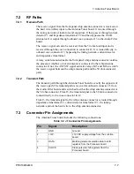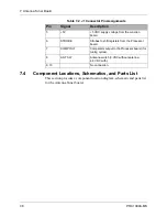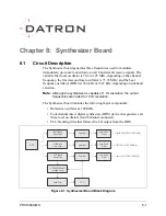
8: Synthesizer Board
8-2
PRC1099A-MS
8.1.1
Reference Oscillator
Temperature-compensated crystal oscillator (TCXO) Y1 provides a 100 MHz
reference frequency for the DDS synthesizer with a standard frequency
tolerance of 1 ppm over temperature. It includes a fine adjustment to allow
centering of the oscillator’s frequency at the time of synthesizer calibration.
The complete frequency determination of the entire transceiver is locked to
this reference, giving the output frequency a stability equal to that of the
TCXO. An in-line 1:1 balun transformer converts the single-ended oscillator
output to a balanced input for the DDS.
8.1.2
Direct Digital Synthesizer (DDS)
The Direct Digital Synthesizer (DDS) generates two local oscillator
frequencies: LO1 and LO2, that are routed to the Mixer board where they
either up-convert or down-convert the transmit or receive frequency. The DDS
receives channel frequency data from the processor over SPI serial data lines.
The BFO (beat frequency oscillator) output (1647 or 1650 kHz) is routed to
the Audio/Filter board where it is modulated by the transmit audio. The BFO
is also used to demodulate the receive signal leaving just the receive audio.
The 4-channel DDS produces all the local oscillator outputs, including the
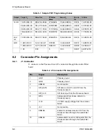
BFO. The BFO is generated in channel 2, the first LO (76.6 to 105 MHz) is
generated in channel 1, and the second LO (73.35 MHz) is generated by
channel 0. The fourth channel is unused.
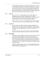
The DDS operates all three local oscillators at the appropriate frequency. The
device is tuned by inputting a 32-bit digital tuning word expressed by:
8.1.3
PLL/Tracking Filter
The first LO uses a phase-locked loop (PLL) circuit that filters the output of
the DDS first local oscillator (LO1) to remove any wide-band spurious signals
and noise. The loop filter of the PLL is composed of U17, R101, R102 and
R133 together with C121, C123, C124, and C125. The output of U17 controls
the frequency of VCO U16.
The PLL circuit also tracks the LO1 output frequency exactly using low-noise
VCO U16 so there is no additional division noise commonly associated with
phase locked loops.
F
o
= (FTW)(Fs)/2
32
where:
F
o
= DDS output frequency
0<= FTW <= 2
31
FTW = Frequency tuning word
Fs = System clock rate
Содержание PRC1099A
Страница 4: ......
Страница 8: ......
Страница 35: ......
Страница 49: ...3 Audio Filter Board 3 14 PRC1099A MS Figure 3 2 Audio Filter Board Component Locations 738221 Rev J ...
Страница 65: ......
Страница 71: ...4 1650 kHz IF Board 4 6 PRC1099A MS Figure 4 2 1650 kHz IF Board Component Locations 738028 Rev D ...
Страница 76: ......
Страница 86: ...5 Mixer Board 5 10 PRC1099A MS Figure 5 4 Mixer Board Component Locations 738217 Rev H ...
Страница 97: ......
Страница 103: ...6 Power Amplifier Board 6 6 PRC1099A MS Figure 6 2 Power Amplifier Board Component Locations 738617 Rev C ...
Страница 117: ...7 Antenna Tuner Board PRC1099A MS 7 9 Figure 7 2 Antenna Tuner Driver Board Component Locations 738346 Rev B ...
Страница 118: ...7 Antenna Tuner Board 7 10 PRC1099A MS Figure 7 3 Antenna Tuner Board Component Locations 738027 Rev D ...
Страница 125: ......
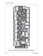
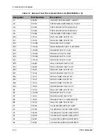
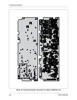
Страница 131: ...8 Synthesizer Board 8 6 PRC1099A MS Figure 8 2 Synthesizer Board Component Locations 738025 Rev A ...
Страница 163: ...9 Processor Board 9 14 PRC1099A MS Figure 9 2 Processor Board Component Locations 738218 Rev B ...
Страница 178: ...10 Display Board 10 8 PRC1099A MS Figure 10 1 Display Board Component Location Diagram 738220 Rev G ...
Страница 181: ......
Страница 185: ...11 Junction Board 11 4 PRC1099A MS Figure 11 1 Junction Board Component Locations 738222 Rev F ...
Страница 200: ......
Страница 207: ...13 Internal Options PRC1099A MS 13 7 Figure 13 3 ALE Board Component Locations 1 of 2 738215 Rev B ...
Страница 208: ...13 Internal Options 13 8 PRC1099A MS Figure 13 4 ALE Board Component Locations 2 of 2 738215 Rev B ...
Страница 241: ......
Страница 247: ...Index 6 T Technical specifications 1 2 Transmit path 2 4 U USB 1 4 see also Modulation modes USB LSB mode V VSWR 1 4 ...


