ADV
ANCEINFORMA
TION
R2
C1
R3
C3
From PFD /
Charge Pump
>>
>>
LF1 / LF2
LMK05028
C2
R4
C4
Copyright © 2018, Texas Instruments Incorporated
32
SNAS724 – FEBRUARY 2018
Product Folder Links:
Copyright © 2018, Texas Instruments Incorporated
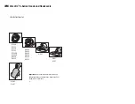
9.3.8.6 APLL Loop Filter
Each APLL supports programmable loop bandwidth from 100 kHz to 1 MHz. The analog loop filter components,
R2, C1, R3, C3, R4, and C4 can be configured through registers. C2 for each APLL is an external 0.1-µF
capacitor on the LF1 or LF2 pins. Because each APLL operates in fractional mode during normal operation, the
charge pump non-linearity should be reduced by configuring the bleed resistor.
shows the APLL loop
filter structure between the PFD/charge pump output and VCO input.
Figure 27. Loop Filter Structure of Each APLL
9.3.8.7 APLL Fractional Feedback Divider (NDIV)
The fractional feedback divider (NDIV) of each APLL includes a 9-b integer portion (INT), 40-b numerator portion
(NUM), and 40-b denominator portion (DEN). The total NDIV value is: NDIV = INT + NUM / DEN. The NDIV
output sets the APLL PFD frequency, which should be equal to the XO doubler output frequency.
9.3.8.8 REF-DPLL Reference Divider (RDIV)
The reference clock input paths to each REF-DPLL features a 16-b reference divider (RDIV) for each clock input
(IN0 to IN3). The output of each RDIV sets the frequencies to the reference input mux and the TDC rate of the
REF-DPLL. There are also two additional RDIV for the internal VCO loopback clocks (IN4 and IN5) which could
be used in cascaded DPLL configurations. IN4 refers to the VCO1 loopback clock to DPLL2 reference input, and
IN5 refers to the VCO2 loopback clock to DPLL1 reference input.
9.3.8.9 TCXO Input Doubler (D) and Divider (MDIV)
The TCXO input features a frequency doubler followed by a 5-b divider (MDIV). The MDIV output is sent to both
TCXO-DPLLs and sets the TDC rate for both TCXO-DPLLs if used in the configuration.
9.3.8.10 REF-DPLL and TCXO-DPLL Time-to-Digital Converter (TDC)
Each REF-DPLL and TCXO-DPLL TDC operates up 30 MHz. The TDC resolution is fine enough to achieve in-
band phase noise of –102 dBc/Hz at 100-Hz offset for a 122.88-MHz output. The REF-DPLL TDC rate is: REF-
TDC = F
INx
/ RDIVx. . The TCXO-DPLL TDC rate is: TCXO-TDC = F
TCXO
× D / MDIV, where D = 1 (doubler
disabled) or 2 (enabled).
9.3.8.11 REF-DPLL and TCXO-DPLL Loop Filter
Each REF-DPLL and TCXO-DPLL supports programmable loop bandwidth from 10 mHz to 4 kHz and can
achieve jitter peaking below 0.1 dB. The jitter transfer characteristic of each DPLL attenuates the noise of its
respective input clock at –60 dB/decade slope above its configured loop bandwidth.
In 2-loop mode with the REF-DPLL , the TCXO-DPLL is bypassed and the REF-DPLL loop filter output directly
modulates the APLL NDIV MASH engine to steer the APLL VCO into lock with the selected REF-DPLL input.
Summary of Contents for LMK05028
Page 57: ......