background image

5-55

5-4. SERVICE MODE

4-1.

ADJUSTMENT REMOTE COMMANDER

The adjustment remote commander is used for changing the
calculation coefficient in signal processing, EVR data, etc. The
adjustment remote commander performs bi-directional
communication with the unit using the remote commander signal
line (LANC). The resultant data of this bi-directional communication
is written in the non-volatile memory.

1. Using the adjustment remote commander

1)

Connect the adjustment remote commander to the LANC
terminal.

2)

Set the HOLD switch of the adjustment remote commander to
“HOLD” (SERVICE position). If it has been properly
connected, the LCD on the adjustment remote commander will
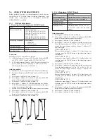
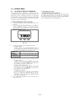
display as shown in Fig. 5-4-1.

Fig. 5-4-1

3)

Operate the adjustment remote commander as follows.
• Changing the page

The page increases when the EDIT button is
pressed, and decreases when the EDIT SEARCH– button is
pressed. There are altogether 16 pages, from 0 to F.

• Changing the address

The address increases when the FF (

)

) button is pressed,

and decreases when the REW (

0

) button is pressed. There

are altogether 256 addresses, from 00 to FF.

• Changing the data (Data setting)

The data increases when the PLAY (

(

) button is pressed,

and decreases when the STOP (

p

) button is pressed. There

are altogether 256 data, from 00 to FF.

• Writing the adjustment data

The PAUSE button must be pressed to write the adjustment
data (C, D, F page) in the nonvolatile memory. (The new
adjusting data will not be recorded in the nonvolatile memory
if this step is not performed.)

4)

After completing all adjustments, turn off the main power
supply (8.4V) once.

Page

Data

Address

Hexadecimal
notation

LCD Display

Decimal notation
conversion value

0 1 2 3 4 5 6 7 8 9 A B C D E F

0 1 2 3 4 5 6 7 8 9 A b c d E F

0 1 2 3 4 5 6 7 8 9 10 11 12 13 14 15

2. Precautions upon using
    the adjustment remote commander

Mishandling of the adjustment remote commander may erase the
correct adjustment data at times. To prevent this, it is recommended
that all adjustment data be noted down before beginning adjustments
and new adjustment data after each adjustment.

Summary of Contents for Handycam Vision DCR-TRV5

Page 1: ...Model Tourist Model DCR TRV5 TRV5E SERVICE MANUAL DIGITAL VIDEO CAMERA RECORDER MICROFILM C MECHANISM Photo DCR TRV5E RMT 809 For MECHANISM ADJUSTMENTS refer to the DV MECHANICAL ADJUSTMENT MANUAL C MECHANISM 9 974 050 11 NTSC model DCR TRV5 PAL model DCR TRV5E SPECIFICATIONS Continued on next page ...

Page 2: ...eck the interboard wiring to ensure that no wires are pinched or contact high wattage resistors 3 Look for unauthorized replacement parts particularly transistors that were installed during a previous repair Point them out to the customer and recommend their replacement 4 Look for parts which through functioning show obvious signs of deterioration Point them out to the customer and recommend their...

Page 3: ...emoval of F Panel Assembly MA 330 Board FP 691 Board and FP 695 Board 2 1 2 2 Removal of Rear Cover Assembly FP 694 Board and Control Switch Block FK4680 PS4680 2 2 2 3 Removal of Mechanism Chassis Block 2 2 2 4 Removal of VC 207 Board Zoom Lens AU 204 Board and DD 110 Board 2 3 2 5 Removal of EVF Block 2 3 2 6 Removal of CD 193 Board 2 4 2 7 Removal of LCD Block 2 5 2 8 Service Position Adjustmen...

Page 4: ...ce Adjustment PD 100 board 5 25 Arrangement Diagram for Adjustment Parts 5 26 5 2 Mechanism Section Adjustment 5 29 2 1 Operating without Cassette 5 29 2 2 Tape Path Adjustment 5 29 1 Preparations for Adjustment 5 29 5 3 Video Section Adjustments 5 30 3 1 Preparations before Adjustments 5 30 3 1 1 Equipment Required 5 30 3 1 2 Precautions on Adjusting 5 31 3 1 3 Adjusting Connectors 5 31 3 1 4 Con...

Page 5: ... 6 Record of Use check 5 60 6 REPAIR PARTS LIST 6 1 Exploded Views 6 1 6 1 1 Front Panel Cabinet L Section 6 1 6 1 2 Rear Cover Cabinet R Section 6 2 6 1 3 LCD Panel Section 6 3 6 1 4 Lens EVF Section 6 4 6 1 5 Cassette Compartment Drum and Reel Table Assembly 6 5 6 1 6 Tape Guide Pinch Slider Assembly and Brake Slider Assembly 6 6 6 1 7 Each Gears and Loading Capstan Motor Assembly 6 7 6 2 Electr...

Page 6: ...witch to the ADJ side Method 2 Use the AC power adaptor 2 HOW TO TAKE A CASSETTE OUT WHEN THE MAIN POWER CANNOT BE TURNED ON Note To take a cassette out forcibly as follows when the main power cannot be turned on remove the cabinet L assembly Apply 4 5 V power from an external power supply to the loading motor as shown below Refer to sections 2 1 and 2 2 for the procedure to remove the cabinet L a...

Page 7: ...y Method While pressing the STOP EXPOSURE key set the switch from OFF to VTR or PLAYER and continue pressing the STOP EXPOSURE key for 5 seconds continuously The service mode will be displayed and the counter will show the backup No and the 5 character self diagnosis codes 3 2 Switching of Backup No By rotating the control dial past self diagnosis codes will be shown in order The backup No in the ...

Page 8: ...ng Load the tape again and perform operations from the beginning Load the tape again and perform operations from the beginning Load the tape again and perform operations from the beginning Load the tape again and perform operations from the beginning Load the tape again and perform operations from the beginning Load the tape again and perform operations from the beginning Load the tape again and p...

Page 9: ...1 1 DCR TRV5 TRV5E SECTION 1 GENERAL This section is extracted from instruction manual DCR TRV5E model ...

Page 10: ...1 2 ...

Page 11: ...1 3 ...

Page 12: ...1 4 ...

Page 13: ...1 5 ...

Page 14: ...1 6 ...

Page 15: ...1 7 ...

Page 16: ...1 8 ...

Page 17: ...1 9 ...

Page 18: ...1 10 ...

Page 19: ...1 11 ...

Page 20: ...1 12 ...

Page 21: ...1 13 ...

Page 22: ...1 14 ...

Page 23: ...1 15 ...

Page 24: ...1 16 ...

Page 25: ...1 17 ...

Page 26: ...1 18 ...

Page 27: ...1 19 ...

Page 28: ...1 20 ...

Page 29: ...1 21 ...

Page 30: ...1 22 ...

Page 31: ...1 23 ...

Page 32: ...1 24 ...

Page 33: ...1 25 ...

Page 34: ...1 26 ...

Page 35: ...1 27 ...

Page 36: ...1 28 ...

Page 37: ...1 29E ...

Page 38: ...to PD 100 board 2 7 LCD block Remove to LCD901 ND901 replaceable 2 5 EVF block Remove 1 to 2 VF 124 board replaceable 5 From CN7001 8 From CN8601 Push the claw Remove the board 7 MA 330 board from CN7000 9 M1 7 2 M1 7 2 M1 7 2 M1 7 2 M1 7 2 1 M1 7 4 1 M1 7 4 1 M1 7 4 3 M1 7 4 º MA 330 board 4 VC 207 board from CN003 FP 691 flexible board S retainer FP 695 flexible board 6 F panel assembly 2 Open t...

Page 39: ...ª FP 694 flexible board Control switch block FK4680 ª FP 694 flexible board 9 FP 694 flexible board from CN003 7 VC 207 board from CN007 Photo retainer M1 7 4 a a 2 3 Cassette lid assembly 1 Stepped special head machine screw 4 M1 7 4 4 M1 7 4 7 Stepped screws 9 Stepped screw º MD frame lower assembly 8 VC 207 board from CN2701 video head 8 VC 207 board from CN3103 drum motor 6 Cabinet L assembly ...

Page 40: ...om CN012 2 Harness SP 152 from CN013 8 FP 696 flexible board from AU 204 board CN7502 6 FP 697 flexible board from AU 204 board CN7503 º AU 204 board M1 7 2 5 5 Zoom lens VCL 4010VD 9 M1 7 2 5 2 5 REMOVAL OF EVF BLOCK 2 EVF cabinet rear assembly 1 M1 7 2 Remove it carefully so that it must not be caught 3 Move it back once º LCD cushion 4680 Note LCD cushion 4680 Note BLF diffusion plate LCD902 8 ...

Page 41: ...BOARD 2 M1 7 2 3 M1 7 2 5 CD 193 board 4 BTP2 7 1 CD 193 board from CN302 6 Remove soldering 9 Remove soldering 7 Two screw P type2 LOCKACE M1 7 2 8 Zoom motor º Two screw P type2 LOCKACE M1 7 2 Focus motor Zoom lens VCL 4010VD ...

Page 42: ...802 Harness blind tape PD flexible sheet PD 100 board ª From CN5501 ª From CN5804 ª From CN5701 Remove the flexible board connected to the LCD from the cabinet R assembly Harness 4 M1 7 2 6 M2 2 5 2 5 LI 65 board 9 M1 7 2 9 M1 7 2 M1 7 2 ª M1 7 2 M1 7 2 M1 7 2 Harness SP 153 from CN5801 Harness SP 154 from CN5803 Hinge cover lower 3 989 856 01 Melt them by soldering iron or attach them with adhesi...

Page 43: ...to sections 2 1 to 2 7 and connect them as shown below DD 110 board MD FK PS block Work table MA 330 board VC 207 board Blocks Use appropriate boxes or the like to support the VC 207 board lens block LCD block FK PS block and MA 330 board Work table Lens block LCD block CPC 8 jig J 6082 388 A LI 65 board Extension cable J 6082 395 A ...

Page 44: ...ER TIMMING GENERATOR BACK LIGHT GENERATOR FK4680 USER CONTROL VL4680 VOLUME FP 699 FUNCTION KEY VC 207 CAMERA PROCESS FOCUS ZOOM IRIS DRIVE VIDEO OUT REC PB PROCESS RF INTERFACE RGB DECODER BLOCKING ECC TBC CHCD DV SIGNAL PROCESS AUDIO PROCESS MODE CONTROL EVR AUDIO MECHA CON SERVO DD 110 DRUM CAPSTAN PWM DRIVE AU 204 AUDIO PROCESSOR CD 193 CCD IMAGER VF 124 COLOR EVF ...

Page 45: ...DCR TRV5 TRV5E SECTION 3 BLOCK DIAGRAMS 3 1 OVERALL BLOCK DIAGRAM 1 3 1 3 2 3 3 3 4 ...

Page 46: ...DCR TRV5 TRV5E 3 2 OVERALL BLOCK DIAGRAM 2 3 6 3 7 3 8 DCR TRV5 TRV5E ...

Page 47: ...DCR TRV5 TRV5E 3 3 POWER BLOCK DIAGRAM 3 9 3 10 3 11 3 12 3 13E ...

Page 48: ...DCR TRV5 TRV5E SECTION 4 PRINTED WIRING BOARDS AND SCHEMATIC DIAGRAMS 4 1 FRAME SCHEMATIC DIAGRAM 4 1 4 2 4 3 FRAME SCHEMATIC DIAGRAM DCR TRV5 TRV5E ...

Page 49: ...ed Signal name XEDIT EDIT PB XREC PB REC 2 non flammable resistor 1 fusible resistor C panel designation A B Line B B Line J IN OUT direction of B LINE C adjustment for repair Circled numbers refer to waveforms Indicated by the color red Measuring conditions voltage and waveform Voltages and waveforms are measured between the measurement points and ground when camera shoots color bar chart of patt...

Page 50: ...DCR TRV5 TRV5E CD 193 BOARD CAMERA REC 1 IC303 1 2 7 0Vp p 0 9Vp p 7 0Vp p 3 2Vp p H 3 2Vp p H H H H 2 IC303 3 4 3 IC303 8 4 IC303 5 IC303 4 9 4 10 CCD IMAGER CD 193 DCR TRV5 TRV5E ...

Page 51: ...IC2303 D 6 IC2304 D 5 IC2700 E 6 IC2701 F 4 IC2702 F 6 IC2704 F 5 IC3101 D 4 IC3501 B 7 IC3502 B 8 IC6101 E 3 IC3102 D 4 L201 A 5 L203 A 5 L204 B 6 L301 A 7 L1101 A 5 L1103 C 4 L1104 C 4 L2301 E 6 L2703 F 4 L2704 E 5 L2707 E 3 L2708 E 5 L2709 F 4 L3102 E 4 L3504 C 8 L3506 B 8 L6100 F 3 L6101 F 2 Q202 A 8 Q203 A 8 Q204 A 8 Q205 A 8 Q302 A 7 Q303 A 8 Q1101 C 4 Q1102 C 4 Q1103 C 5 Q1105 C 4 Q1106 B 5...

Page 52: ... 10 L202 B 12 L302 B 10 L1001 C 10 L1900 C 14 L1901 D 14 L1902 C 15 L2700 F 11 L2705 F 11 L2710 D 12 L2711 D 12 L3100 E 15 L3101 D 12 L3103 E 15 L3505 D 12 L7901 D 16 L7902 D 16 Q301 B 10 Q1001 C 11 Q1002 C 11 Q1003 C 11 Q2706 E 11 Q2707 E 11 Q3100 E 14 Q3101 E 14 Q3102 E 14 R004 A 9 R010 C 13 R205 A 12 R206 A 12 R208 A 12 R209 B 13 R210 A 12 R211 A 12 R212 B 12 R215 B 12 R217 B 12 R218 A 11 R219 ...

Page 53: ...CL202 CAMERA REC PB 3 IC202 2 CAMERA REC 4 IC202 CAMERA REC 5 IC207 º X202 CAMERA REC PB 6 IC205 2 CAMERA REC PB 7 IC209 CAMERA REC 8 IC209 CAMERA REC H 2 8Vp p V 9 IC209 CAMERA REC º IC204 FB204 CAMERA REC PB 2 8Vp p 2V 2 7Vp p 14 26MHz 4 20 4 21 4 22 CAMERA PROCESS VC 207 1 15 For Schematic Diagram Refer to page 4 12 for printed wiring board DCR TRV5 TRV5E ...

Page 54: ...DCR TRV5 TRV5E DCR TRV5 TRV5E 4 23 4 24 FOCUS ZOOM IRIS DRIVE VC 207 2 15 For Schematic Diagram Refer to page 4 12 for printed wiring board ...

Page 55: ...8 3 0Vp p 6 75MHz NTSC PAL Q1102 E CAMERA REC Q112 E PB FL1102 3 CAMERA REC FL1102 3 PB 0 45Vp p H 0 36Vp p H Q112 E PB 480mVp p H 0 13Vp p H 0 14Vp p H 4 26 4 27 4 28 VIDEO OUT VC 207 3 15 For Schematic Diagram Refer to page 4 12 for printed wiring board ...

Page 56: ...3 2Vp p IC2702 PB IC2703 2 3 6 7 CAMERA REC ª IC2703 CAMERA REC º IC2703 CAMERA REC IC2704 2 PB 3 3msec 0 26Vp p 41 8MHz 6 6msec 3 3msec IC2704 º PB 20nsec div 1V div 3 3msec 1 7Vp p 3 3msec 2 8Vp p IC2703 CAMERA REC PB 6 6msec 0 4Vp p 6 0msec IC2703 ª PB NTSC IC2703 ª PB 0 3Vp p 6 7msec PAL 4 29 4 30 4 31 4 32 REC PB PROCESS VC 207 4 15 ...

Page 57: ...DCR TRV5 TRV5E DCR TRV5 TRV5E VC 207 BOARD 5 15 IC6101 ª L6101 REC PB 2 6Vp p 41 85MHz 4 35 4 36 RF INTERFACE VC 207 5 15 For Schematic Diagram Refer to page 4 12 for printed wiring board ...

Page 58: ...R TRV5 TRV5E VC 207 BOARD 6 15 CAMERA REC Q1001 2 0 22Vp p 0 23Vp p Q1002 2 H H Q1003 2 0 15Vp p H 4 37 4 38 4 39 RGB DECODER VC 207 6 15 For Schematic Diagram Refer to page 4 12 for printed wiring board ...

Page 59: ...TRV5E VC 207 BOARD 7 15 CAMERA REC PB IC3500 8 3 0Vp p NTSC 1 0Vp p PAL 1 3Vp p 6MHz IC3502 24 57MHz 4 40 4 41 4 42 DV SIGNAL PROCESS VC 207 6 15 For Schematic Diagram Refer to page 4 12 for printed wiring board ...

Page 60: ...DCR TRV5 TRV5E 4 43 4 44 4 45 4 46 BLOCKING VC 207 8 15 For Schematic Diagram Refer to page 4 12 for printed wiring board ...

Page 61: ...DCR TRV5 TRV5E DCR TRV5 TRV5E 4 48 4 49 4 50 ECC TBC CHCD VC 207 9 15 For Schematic Diagram Refer to page 4 12 for printed wiring board ...

Page 62: ... 2 5Vp p 3 0Vp p 2 9Vp p 13 5MHz 2 0Vp p º IC1900 X1900 IC1900 L1902 IC1900 ª R1914 IC1900 L1901 27MHz NTSC 13 5MHz PAL 11 74MHz 13 5MHz NTSC 36 2MHz PAL 38 5MHz 4 51 4 52 4 53 AUDIO SIGNAL PROCESS VC 207 10 15 For Schematic Diagram Refer to page 4 12 for printed wiring board ...

Page 63: ... C7918 NTSC 1 2Vp p PAL 1 5Vp p 1 7Vp p 1 7Vp p 24 57MHz IC7903 R7903 IC7903 L7902 24 57MHz NTSC REC 31 3MHz PB 24 57MHz PAL REC 31 9MHz PB 26 1MHz 4 54 4 55 4 56 AUDIO DISPLAY VC 207 11 15 For Schematic Diagram Refer to page 4 12 for printed wiring board ...

Page 64: ...DCR TRV5 TRV5E DCR TRV5 TRV5E 4 57 4 58 MODE CONTROL VC 207 12 15 For Schematic Diagram Refer to page 4 12 for printed wiring board ...

Page 65: ...DCR TRV5 TRV5E 4 60 4 61 4 62 EVR AUDIO VC 207 13 15 AV JACK FP 691 For Schematic Diagram Refer to page 4 12 for printed wiring board ...

Page 66: ...C3102 CAMERA REC PB IC3102 REC PB IC3102 º REC PB IC3102 REC PB ª IC3103 REC PB º IC3103 ª REC PB IC3103 REC PB IC3103 REC PB IC3104 2 REC PB 2 2Vp p 13 2msec 13 5MHz 0 1Vp p 1 1msec 2 8Vp p 1 1msec 0 23Vp p 1 1msec 900kHz 900kHz 2 6Vp p 0 92msec 40mVp p 0 92msec 40mVp p 80msec 0 9Vp p 80msec 2 2Vp p 1 1msec 4 63 4 64 4 65 4 66 MECHA CON SERVO VC 207 14 15 For Schematic Diagram Refer to page 4 12 ...

Page 67: ...RV5E VC 207 BOARD 15 15 CAMERA REC PB IC2302 º NTSC 2 9Vp p PAL 2 6Vp p 2 3Vp p 20MHz IC2302 32 7kHz 4 67 4 68 4 69 4 70 MODE CONTROL VC 207 15 15 For Schematic Diagram Refer to page 4 12 for printed wiring board ...

Page 68: ...TERY FP 594 LOADING MOTOR SENSORS SWITCHES PRINTED WIRING BOARDS Ref No LI 65 Board 10 000 Series FP 594 Flexible Board 9 800 Series 4 71 For Printed wiring board Refer to page 4 65 for FP 594 schematic diagram ...

Page 69: ...4 72 LOADING MOTOR FP 594 LI 65 BOARD BT001 B 1 CN001 A 2 BATTERY LI 65 For printed wiring boards There are few cases that the part printed on this diagram isn t mounted in this model ...

Page 70: ...7577 B 1 C7578 B 1 CN7502 A 1 CN7503 A 2 D7502 A 3 D7503 A 4 D7504 A 1 D7506 B 4 D7507 B 4 D7508 B 4 D7510 B 1 D7511 A 1 D7512 A 1 D7513 B 1 D7514 B 4 FB7501 B 3 IC7501 A 3 IC7502 A 1 IC7504 B 3 IC7508 B 1 L7501 B 2 L7505 B 3 Q7501 B 2 Q7502 B 2 Q7506 A 1 Q7507 B 2 Q7511 B 2 Q7513 B 1 Q7514 A 1 R7501 B 2 R7502 B 2 R7503 A 3 R7504 A 3 R7505 A 4 R7506 A 4 R7507 A 4 R7508 A 1 R7509 B 4 R7510 A 4 R751...

Page 71: ...DCR TRV5 TRV5E 4 75 4 76 4 77 AUDIO PROCESSOR AU 204 ...

Page 72: ... 3 D7002 A 3 D8651 A 3 D8652 B 1 IC7000 F 2 IC8401 F 3 IC8402 F 3 IC8651 B 1 J7000 B 4 L7000 E 2 L8402 F 3 L8403 A 3 L8404 A 3 L8405 F 3 Q7000 B 2 Q8401 A 3 Q8601 D 3 Q8603 D 2 Q8604 D 2 Q8605 D 1 Q8606 D 1 Q8651 B 2 R7000 A 4 R7001 A 3 R7004 B 3 R7005 A 2 R7006 F 2 R7007 F 1 R7008 F 1 R7013 A 2 R7014 B 2 R7016 A 2 R7017 A 2 R7018 A 2 R7020 B 1 R7021 B 2 R7022 B 2 R7023 A 2 R8401 B 2 R8403 B 2 R84...

Page 73: ...DCR TRV5 TRV5E 4 81 4 82 AUDIO PROCESS IR TRANSMMITER MA 330 ...

Page 74: ...9 D 6 Q5701 B 2 Q5702 D 3 Q5801 A 1 Q5802 A 2 Q5803 A 2 Q5804 A 1 Q5805 D 1 Q5806 A 2 Q5807 A 3 Q5808 A 1 Q5809 D 1 Q5811 B 3 Q5812 A 2 Q5813 B 3 Q5814 A 2 Q5817 A 2 Q5820 A 3 Q5822 A 3 Q5823 A 3 Q5824 A 2 R5501 B 5 R5502 B 5 R5503 B 5 R5504 B 5 R5505 B 5 R5506 B 5 R5507 B 5 R5508 B 5 R5509 B 5 R5510 A 5 R5511 A 5 R5512 B 5 R5513 B 6 R5514 A 5 R5515 A 5 R5516 B 6 R5517 B 6 R5518 B 6 R5520 A 5 R552...

Page 75: ...OARD 1 3 PB 1 IC5502 8 PB 0 26Vp p 0 32Vp p 0 25Vp p 3 8Vp p 2H 3 8Vp p 3 8Vp p H H 2H 2H 2 IC5502 9 PB 3 IC5502 º PB 4 IC5502 º PB 5 IC5502 PB 6 IC5502 PB H NTSC PAL 1 IC5502 8 PB 0 48Vp p H 4 85 4 86 RGB DECODER PD 100 1 3 ...

Page 76: ...DCR TRV5 TRV5E 4 87 4 88 TIMMING GENERATOR PD 100 2 3 For Schematic Diagram Refer to page 4 83 for printed wiring board Refer to page 4 86 for waveform ...

Page 77: ...DCR TRV5 TRV5E 4 89 4 90 BACK LIGHT GENERATOR PD 100 3 3 For Schematic Diagram Refer to page 4 83 for printed wiring board Refer to page 4 86 for waveform ...

Page 78: ...205 I 3 C5206 H 3 C5207 H 3 C5208 H 4 C5209 C 4 CN5001 I 2 CN5202 E 1 D5101 C 4 D5102 H 2 D5201 C 4 D5202 H 7 IC5001 H 1 IC5002 B 1 IC5101 C 4 IC5102 C 2 L5001 I 1 L5002 C 1 L5101 C 4 L5102 C 2 L5103 C 2 L5201 I 3 L5202 H 4 ND5201 I 7 Q5101 C 3 Q5102 C 3 Q5103 C 3 Q5104 C 3 Q5201 H 4 R5005 B 1 R5008 B 1 R5009 B 1 R5020 I 1 R5021 I 1 R5022 I 1 R5023 I 1 R5024 B 1 R5025 B 2 R5026 B 1 R5030 H 1 R5031...

Page 79: ...0 34Vp p 0 25Vp p 7Vp p 2H 7Vp p 7Vp p 11Vp p H 2 6Vp p H H 2H 2H 2 IC5001 9 PB 3 IC5001 º PB 4 IC5001 º PB 5 IC5001 PB 6 IC5001 PB 7 IC5101 8 IC5102 H PAL 1 IC5502 8 PB 0 48Vp p H NTSL 11 06MHz PAL 10 97MHz 4 93 4 94 4 95 4 96 COLOR EVF VF 124 1 2 2 2 ...

Page 80: ...DCR TRV5 TRV5E DCR TRV5 TRV5E DD 110 BOARD CAMERA REC PB 1 IC801 0 9Vp p NTSC 2 2µsec PAL 2 0µsec 4 98 4 99 4 100 DRUM CAPSTAN PWM DRIVE DD 110 ...

Page 81: ...805 D 3 L806 D 3 L807 E 3 L808 D 3 L809 D 3 L810 A 1 L811 B 1 L812 B 1 L813 B 1 L814 A 2 L815 A 1 L816 A 2 L817 A 1 L818 A 1 L819 A 1 L820 B 2 L821 A 1 L822 C 3 PS001 B 4 PS002 B 4 PS003 B 4 PS004 B 4 Q802 A 3 Q803 A 3 Q804 B 3 Q805 B 3 Q807 A 3 Q809 B 3 Q810 B 3 Q812 B 3 Q817 B 1 Q818 B 2 Q819 D 1 Q823 C 1 Q825 D 2 Q829 D 1 Q830 D 1 Q841 D 2 Q843 D 1 Q844 D 1 Q852 D 2 Q853 D 2 Q854 D 1 Q859 D 1 R...

Page 82: ...e ADJ side Ref No J 1 J 2 J 3 J 4 J 5 J 6 J 7 J 8 J 9 J 10 J 11 J 12 Name Filter for color temperature correction C14 ND filter 1 0 ND filter 0 3 Pattern box PTB 450 Color chart for pattern box Adjustment remote commander RM 95 upgraded Note 1 Siemens star chart Clear chart for pattern box Multi CPC jig CPC 8 jig Extension cable 80P 0 4mm Power code Note 2 IR receiver jig Parts Code J 6080 058 A J...

Page 83: ...on time etc will be lost Before removing note down the self diagnosis data and the data on history use data of page 2 address 35 to 3D Refer to the Service Mode for the data on the history use Note 4 Setting the Forced Camera Power ON Mode 1 Select page 0 address 01 and set data 01 2 Select page D address 10 set data 01 and press the PAUSE button of the adjustment remote commander The above proced...

Page 84: ... power adaptor 8 4Vdc Extension cable 80P 0 4m J 6082 395 A FP 698 CN5701 CN5501 CN5601 CN5802 CN5801 CN5803 FP 699 J 6082 388 A Must be connected when performing the video system or color EVF system adjustments Need not connected when performing the camera system adjustment Vectorscope AUDIO L White AUDIO R Red VIDEO Yellow Color monitor Must be connected when connecting the vectorscope and color...

Page 85: ...w Cyan Green White Magenta Red Blue Color bar chart standard picture frame Fig a Video output terminal output waveform Fig b TV monitor picture Adjust the camera zoom and direction to obtain the output waveform shown in Fig a and the TV monitor display shown in Fig b Fig 5 1 4 3 Subjects 1 Color bar chart Standard picture frame When performing adjustments using the color bar chart adjust the pictu...

Page 86: ...Modification of F Page Data Initializing Method 1 Select page 6 address 00 and set data 01 2 Select page 6 address 01 set data 2D NTSC or data 2F PAL and press the PAUSE button of the adjustment remote commander 3 Select page 6 address 03 set data 01 and press the PAUSE button of the adjustment remote commander 4 Wait for more than 2 seconds and select page 6 address 02 and check that the data is ...

Page 87: ...ata 2 Fixed data 1 Initialized data Fixed data 2 Fixed data 1 Fixed data 2 Fixed data 1 Address 7A 7B 7C 7D 7E 7F 80 81 82 83 84 85 86 87 88 89 8A 8B 8C 8D 8E 8F 90 91 92 93 94 95 96 97 98 99 9A 9B 9C 9D 9E 9F A0 A1 A2 A3 A4 A5 A6 A7 A8 A9 AA AB AC AD AE AF B0 B1 Initial value NTSC FF EE PAL FF EE Remark Fixed data 1 Fixed data 2 Fixed data 1 Fixed data 2 Modified data copy the data built in the s...

Page 88: ...AL Remark Fixed data 1 Initialized data Fixed data 2 Fixed data 1 Fixed data 2 Fixed data 1 Fixed data 2 Fixed data 1 Fixed data 2 Modified data copy the data built in the same model Fixed data 1 Initialized data Fixed data 2 Fixed data 1 Initialized data Address EA EB EC ED EE EF F0 F1 F2 F3 F4 F5 F6 F7 F8 F9 FA FB FC FD FE FF Initial value NTSC PAL Remark Fixed data 1 Initialized data Table 5 1 ...

Page 89: ...2 or Pin of IC201 or Pin 2 of IC205 Frequency counter F 1C CL202 f 18000000 90Hz NTSC f 18000000 90Hz PAL Pin 2 of IC205 f 27000000 135Hz NTSC f 27000000 135Hz PAL Note Perform GUM PLL Adjustment befor this adjustment Adjusting method 1 Select page 6 address 00 and set data 01 2 Select page F address 1C change the data and set the clock frequency f to the specified value 3 Press the PAUSE button o...

Page 90: ...l decimal Conversion Table of 5 4 Service mode 16 Calculate X1 using the following equations decimal notation calculation A W2 K1 W1 K2 Equation 1 B W1 K1 Equation 2 X1 1840 48 A 16 B A Equation 3 17 Convert X1 to hexadecimal notation and obtain X1 Round off to one decimal place 18 Select page F address 1E set data X1 and press the PAUSE button 19 Select page 6 address 01 and set data 01 and press...

Page 91: ...pleting Adjustments 1 Turn OFF the main power supply 8 4V 2 Perform Flange Adjustment 2 Address 24 25 26 27 28 29 Data 4A 15 90 19 84 13 Address 38 39 3A 3B 3C Data 20 00 19 00 1D 5 2 Flange Back Adjustment 2 Perform this adjustment after performing Flange BackAdjustment 1 Subject Subject more than 500m away Subjects with clear contrast such as buildings etc Measurement Point Check operation on TV...

Page 92: ...n be checked if it is focused or not by observing the data on the pageA of the adjustment remote commander 1 Select page 6 address 04 and set data 0F 2 Page A shows the state of the focus A 00 XX Odd Focused Even Unfocused Processing after Completing Adjustments 1 Select page 6 address 04 and set data 00 2 Select page 6 address 21 and set data 00 7 Picture Frame Setting Subject Color bar chart sta...

Page 93: ...nd press the PAUSE button of the adjustment remote commander 4 Adjust the GAIN and PHASE of the vectorscope and adjust the burst luminance point to the burst position of the color reproduction frame 5 Change the data of page F address 2E 30 8F and 90 and settle each color luminance point in each color reproduction frame Note Be sure to press the PAUSE button of the adjustment remote commander befo...

Page 94: ...ble 5 4 1 Hexadecimal notation decimal notation conversion table of 5 4 Service mode 9 Calculate D3 using the following equations Equations 1 and 2 are for decimal notation calculation When D2 D0 D3 D1 21 Equation 1 When D2 D0 D3 D1 22 Equation 2 10 Convert D3 to hexadecimal notation and obtain D3 11 Select page F address 36 set data D3 and press the PAUSE button of the adjustment remote commander...

Page 95: ...asurement Point DDS display of LCD or TV monitor Measuring Instrument Note Adjustment Page F Adjustment Address 2C Specified Value 70 to 78 NTSC 6C to 74 PAL Note The right two digits of the display data at the right bottom side of the LCD and TV monitor is the object data CA 00 00XX Object data Switch setting 1 STEADY SHOT Menu display OFF Adjusting method 1 Select page 0 address 01 and set data ...

Page 96: ... button of the adjustment remote commander Processing after Completing Adjustments 1 Select page D address 11 and set data 10 and press the PAUSE button of the adjustment remote commander 2 Select page 0 address 01 and set data 00 3 Select page 6 address 00 and set data 00 4 Select page 6 address 01 and set data 00 and press the PAUSE button of the adjustment remote commander 5 Select page 6 addre...

Page 97: ...sensor incorporates a precision oscillator Handle it with care as if it dropped the balance of the oscillator will be disrupted and operations will not be performed properly Adjustment Page F Adjustment Address 41 42 Note The sensor sensitivity of SE301 and SE302 of the CD 193 board is written only on the repair parts Adjusting method 1 Select page 6 address 00 and set data 01 2 Read the sensor se...

Page 98: ... IN BL 4 75 BL 4 75 VCO EVF VG 1 EVF Initial Data Input Mode VTR stop Signal No signal Adjustment Page D Adjustment Address 70 to 77 79 7A 87 to 8F 99 Adjusting method 1 Select page 0 address 01 and set data 01 2 Select page D and input the data in the following table Note To write in the non volatile memory EEPROM press the PAUSE button of the adjustment remote commander each time to set the data...

Page 99: ...of CN005 EVF VG on VC 207 board Measuring Instrument Oscilloscope Adjustment Page D Adjustment Address 7A Specified Value A 7 1 0 1V Adjusting method 1 Select page 0 address 01 and set data 01 2 Select page 2 address 11 set data 04 and press the PAUSE button of the adjustment remote commander 3 Input the following data to page D address 88 to 8D Note Press the PAUSE button of the adjustment remote...

Page 100: ...USE button of the adjustment remote commander each time to set the data 7 Select page 2 address 11 set data 00 and press the PAUSE button of the adjustment remote commander 8 Select page 0 address 01 and set data 00 Fig 5 1 14 Address Data 88 00 89 27 8A 00 8B 00 8C 00 8D 00 2H White 30 Pedestal A Address Data 88 38 89 00 8A 20 8B 20 8C 02 NTSC 00 PAL 8D 00 5 Backlight Consumption Current Adjustme...

Page 101: ...page D address 71 and 72 set the data to the initial value Note Press the PAUSE button of the adjustment remote commander each time to set the data 4 Check that the LCD screen is not colored If colored change the data of page D address 71 and 72 so that the EVF screen is not colored Note To write in the non volatile memory EEPROM press the PAUSE button of the adjustment remote commander each time ...

Page 102: ...6 7 8 9 10 Signal Name XTEST PANEL XHD HSY SYF GND 1 LCD Initial Data Input Mode VTR stop Signal Arbitrary Adjustment Page D Adjustment Address 60 to 67 6A to 6F 80 to 86 8E 8F 99 Adjusting method 1 Select page 0 address 01 and set data 01 2 Select page D and input the data in the following table Note To write in the non volatile memory EEPROM press the PAUSE button of the adjustment remote comman...

Page 103: ...Specified Value T 1 5 0 3µsec NTSC T 3 1 0 3µsec PAL Checking method 1 Check that the delay time T satisfies the specified value Fig 5 1 16 T 1 5V 1 5V PANEL XHD HSY 4 D range Adjustment PD 100 board Set the D range of the RGB decoder used to drive the LCD to the specified value If deviated the LCD screen will become blackish or saturated whitish Mode VTR playback Signal Alignment tape For audio o...

Page 104: ...justment For NTSC model For PAL model Fig 5 1 18 Address Data 82 00 83 00 Address Data 82 20 83 20 White Pedestal A 2H White Pedestal A 2H 6 Contrast Adjustment PD 100 board Set the level of theVIDEO signal for driving the LCD to the specified value If deviated the screen image will be blackish or saturated whitish Mode VTR playback Signal Alignment tape For audio operation check XH5 3 NTSC XH5 3P...

Page 105: ... color saturation to the standard value If deviated the color will be to dark or light Mode VTR playback Signal Alignment tape For audio operation check XH5 3 NTSC XH5 3P PAL Measurement Point Pin 3 of CN5501 VG External trigger Pin 4 of CN5501 PANEL COM Measuring Instrument Oscilloscope Adjustment Page D Adjustment Address 6D Specified Value A 0 15 0 05V NTSC A 0 20 0 05V PAL Adjusting method 1 S...

Page 106: ... data to page D address 82 and 83 Note Press the PAUSE button of the adjustment remote commander each time to set the data 6 Select page 0 address 01 and set data 00 9 V COM Adjustment PD 100 board Set the DC bias of the common electrode drive signal of LCD to the specified value If deviated the LCD display will move producing flicker and conspicuous vertical lines Mode VTR stop Signal No signal M...

Page 107: ...ARRANGEMENT DIAGRAM FOR ADJUSTMENT PARTS VC 207 board SIDE A VC 207 board SIDE B 5 26 ...

Page 108: ... and press the PAUSE button of the adjustment remote commander 3 Select page D address 10 and set data 00 and press the PAUSE button 4 Select page 0 address 01 and set data 00 5 Disconnect the power supply of the unit 2 2 TAPE PATH ADJUSTMENT 1 Preparations for Adjustment 1 Clean the tape running side tape guide capstan shaft pinch roller 2 Connect the adjustment remote commander to the LANC jack ...

Page 109: ...operation check for NTSC XH5 3 Parts code 8 967 997 51 System operation check for NTSC XH5 5 Parts code 8 967 997 61 BIST check for NTSC XH5 6 Parts code 8 967 997 71 Audio operation check for PAL XH5 3P Parts code 8 967 997 55 System operation check for PAL XH5 5P Parts code 8 967 997 66 BIST check for PAL XH5 6P Parts code 8 967 997 76 11 Adjustment remote commander J 6082 053 B 12 CPC 8 jig J 6...

Page 110: ...nd Adjustment To remove disconnect the following connectors VC 207 board CN201 50P 0 5mm 7 AU 207 board Audio circuit needs not be connected except during Audio System Adjustments and IR Transmitter Adjustments To remove disconnected the following connector VC 207 board CN011 39P 0 3mm 8 Use the following extension cable between DD 110 board CN802 and VC 207 board CN010 J 6082 395 A 80P 0 4mm Note...

Page 111: ...Connecting the Equipment Connect the measuring instruments as shown in Fig 5 3 1 and perform the adjustments Adjustment remote commander LANC jack Main unit AUDIO VIDEO jack TV monitor VIDEO Yellow AUDIO L White AUDIO R Red ...

Page 112: ...st signal Horizontal sync signal 0 3V 100 Yellow Cyan Green Magenta Red Blue White Black 1V 0 714V 0 286V White 75 White 100 Yellow Cyan Green Magenta Red Blue Burst signal 0 286V Q I Horizontal sync signal 75 White Yellow Cyan Green Magenta Red Blue Q I White 100 Black For NTSC model For PAL model Color bar signal waveform Color bar pattern Color bar signal waveform Color bar pattern Fig 5 3 2 Co...

Page 113: ... different in destination When changing the data copy the data built in the same model Note If copy the data built in the different model the camcorder may not operate 3 When changing the data press the PAUSE button of the adjustment remote commander each time when setting new data to write the data in the non volatile memory 4 Check that the data of adjustment addresses is the initial value If no...

Page 114: ...j Fixed data 1 Initialized data Fixed data 2 Modified data copy the data built in the same model Fixed data 1 Initialized data Fixed data 2 Address 40 41 42 43 44 45 46 47 48 49 4A 4B 4C 4D 4E 4F 50 51 52 53 54 55 56 57 58 59 5A 5B 5C 5D 5E 5F 60 61 62 63 64 65 66 67 68 69 6A 6B 6C 6D 6E 6F 70 71 72 73 74 75 76 77 Initial value NTSC 79 8A 6A A1 7C 89 8B 8C 79 6E 80 80 77 B0 B0 PAL 79 8A 6A A1 7C 8...

Page 115: ... Page Data If the C Page data has been initialized change the data of the Fixed data 2 address shown in the following table by manual input Modifying Method 1 Before changing the data select page 0 address 01 and set data 01 2 New data for changing are not shown in the tables because they are different in destination When changing the data copy the data built in the same model Note If copy the dat...

Page 116: ...ata 1 Fixed data 2 Fixed data 1 Fixed data 2 Fixed data 1 Fixed data 2 Fixed data 1 Fixed data 2 Fixed data 1 Fixed data 2 Fixed data 1 Emergency memory address PLL fo adj REC current adj AEQ adj AGC center level adj Fixed data 1 PLL capture range adj CLK DELAY adj Fixed data 1 Address 4A 4B 4C 4D 4E 4F 50 51 52 53 54 55 56 57 58 59 5A 5B 5C 5D 5E 5F 60 61 62 63 64 65 66 67 68 69 6A 6B 6C 6D 6E 6F...

Page 117: ...ON SERVICE position 4 Turn on the power supply 5 Load a cassette and set to the camera recording mode 6 Select page 0 address 01 and set data 01 7 Decrease the output voltage of the regulated power supply so that the digital voltmeter display is 5 30 0 01Vdc 8 Select page 2 address 51 read the data and this data is named Dref 9 Select page D address 28 set data Dref and press the PAUSE button of t...

Page 118: ...ns that the T reel FG adjustment has ended normally 15 Select page C address 6A set data 00 and press the PAUSE button of the adjustment remote commander 16 Set the data of page 0 address 01 and set data 00 17 Turn OFF the power supply Measurement Point Measuring Instrument Adjustment Page Adjustment Address Specified Value Adjustment remote commander display data C 59 6F T reel FG Duty Adjustment...

Page 119: ...tment remote commander 10 Select page 0 address 01 and set data 00 Fig 5 3 4 A 0 1 µsec 2 PLL f0 Adjustment VC 207 Board Mode VTR stop Measurement Point Display data of page 3 address 04 Measuring Instrument Adjustment remote commander Adjustment Page C Adjustment Address 3C 3D Specified Value Displayed data is FD to FF or 00 to 03 FF 00 are center values Adjusting method 1 Select page 0 address 0...

Page 120: ...ustment Fig 5 3 5 CH1 CH2 CH1 CH2 EVEN ch EVEN ch 3 33msec When the CH1 pulse is not set When the CH1 pulse is set 4 AGC Center Level Adjustment VC 207 Board Mode Camera recording playback LP mode Subject Arbitrary Signal Playback signal of recorded tape Measurement Point CH1 CL042 Pin 203 of IC1701 C1ERP CH2 Pin 6 of CN005 JSWP Measuring Instrument Oscilloscope Trigger source CH2 Adjustment Page ...

Page 121: ...n 14 Select page C address 5A set data 8C and press the PAUSE button 15 Select page 0 address 01 and set data 00 6 PLL Capture Range Adjustment VC 207 Board Mode Camera recording playback LP mode Subject Arbitrary Signal Playback signal of recorded tape Measurement Point CH1 CL042 Pin 203 of IC1701 C1ERP CH2 Pin 6 of CN005 JSWP Measuring Instrument Oscilloscope Trigger source CH2 Adjustment Page C...

Page 122: ...ss 0E Measuring Instrument Adjustment remote commander Specified Value C0 to FF Adjusting method 1 Select page 0 address 01 and set data 01 2 Select page 2 address 05 set data 02 and press the PAUSE button of the adjustment remote commander 3 Select page D address B0 set data 03 and press the PAUSE button 4 Select page 2 address 0E and check that the data is C0 to FF 5 Select page D address B0 set...

Page 123: ...01 and set data 00 5 Perform Composite Output Chroma Level Adjustment Fig 5 3 8 A H 2 Composite Output Chroma Level Adjustment VC 207 Board Set the chroma signal level of the composite video output signal Mode VTR stop Signal No signal Measurement Point Video signal terminal of AUDIO VIDEO jack 75 Ω terminated Measuring Instrument Oscilloscope Adjustment Page D Adjustment Address 97 Specified Valu...

Page 124: ...et the burst signal level A to the specified value 3 Press the PAUSE button of the adjustment remote commander 4 Select page 0 address 01 and set data 00 Fig 5 3 10 A H 4 S Y Output Level Adjustment VC 207 Board Set the Y signal level of the S video output signal Mode VTR stop Signal No signal Measurement Point Y signal terminal of S VIDEO jack 75 Ω terminated Measuring Instrument Oscilloscope Adj...

Page 125: ...01 01 0A 00 01 0E 00 01 8E 00 Page 4 4 Address 15 14 Data C6 NTSC F8 PAL 90 NTSC 3E PAL 3 5 4 BIST Check 1 Playback System Check 1 Set the POWER switch to VTR or PLAYER position 2 Connect the adjustment remote commander and set the HOLD switch to HOLD SERVICE position 3 Playback the BIST check tape XH5 6 NTSC XH5 6P PAL IC1701 D1 Playback System Check 4 Select page 4 address 11 and set data 04 the...

Page 126: ...ormal following data will be displayed in page 4 address 1A and 1B 20 Only for AEP and UK model select page D address 14 and set the data memorized at step 5 21 Select page D address 15 and set the data memorized at step 6 22 Press the PAUSE button of the adjustment remote commander 23 Select page 0 address 01 and set data 00 Page 4 4 Address 17 16 Data 19 NTSC 2A PAL AA NTSC AE PAL Page 4 4 Addre...

Page 127: ...der 5 Select page 2 address 12 set data 00 and press the PAUSE button of the adjustment remote commander 6 Select page 0 address 01 and set data 00 Main unit IR receiver jig CN003 pin 5 Frequency counter 2 IR Video Deviation Adjustment MA 330 board Mode VTR playback Signal Alignment tape For audio operation check XH5 3 NTSC XH5 3P PAL Measurement Point VIDEO OUT terminal of IR receiver jig Termina...

Page 128: ...page 0 address 01 and set data 01 2 Connect the audio level meter to the AUDIO L terminal of the IR receiver jig 3 Select page D address 92 change the data and set the 400Hz audio signal level to the specified value 4 Press the PAUSE button of the adjustment remote commander 5 Connect the audio level meter to the AUDIO R terminal of the IR receiver jig 6 Check that the 400Hz audio signal level is ...

Page 129: ...devices as shown in Fig 5 3 16 Fig 5 3 16 Recording Camera mode Audio oscillator Attenuator 600 Ω Left Right Main unit MIC 600 Ω 270 Ω 1 249 410 11 330 Ω 1 249 411 11 Main unit AUDIO VIDEO OUT Left White Right 47k Ω 47k Ω Video Yellow TV monitor Audio level meter or Distortion meter 47k Ω 1 249 437 11 Playback Red ...

Page 130: ...t or right terminal of AUDIO VIDEO jack Measuring Instrument Audio distortion meter Specified Value Below 0 4 200Hz to 6kHz BPF ON Checking Method 1 Input the 400Hz 66dBs signal in the MIC jack 2 Record in the camera mode 3 Playback the recorded section 4 Check that the distortion is the specified value 4 Overall Noise Level Check Mode Camera recording and playback Signal No signal Insert a shorti...

Page 131: ...ARRANGEMENT DIAGRAM FOR ADJUSTMENT PARTS VC 207 board SIDE A VC 207 board SIDE B 5 52 ...

Page 132: ...hanging the address The address increases when the FF button is pressed and decreases when the REW 0 button is pressed There are altogether 256 addresses from 00 to FF Changing the data Data setting The data increases when the PLAY button is pressed and decreases when the STOP p button is pressed There are altogether 256 data from 00 to FF Writing the adjustment data The PAUSE button must be press...

Page 133: ...3 84 85 86 87 88 89 90 91 92 93 94 95 96 97 98 99 100 101 102 103 104 105 106 107 108 109 110 111 112 113 114 115 116 117 118 119 120 121 122 123 124 125 126 127 128 129 130 131 132 133 134 135 136 137 138 139 140 141 142 143 144 145 146 147 148 149 150 151 152 153 154 155 156 157 158 174 159 175 160 161 162 163 164 165 166 167 168 169 170 171 172 173 177 176 178 179 180 181 182 183 184 185 186 18...

Page 134: ... data 01 2 Select page 3 address 01 set data FD and press the PAUSE button 3 Select page 0 address 01 and set data 00 Function Normal Forced camera power ON Forced VTR power ON Forced camera VTR power ON Data 00 01 02 03 Contents EMG code when first error occurs Upper MSW code when shift starts when first error occurs Lower MSW code when first error occurs Lower MSW code to be moved when first err...

Page 135: ...EW Code 7 F 5 D 9 E C B 3 Contents Position at which the cassette component lock is released at the farthest unload side mechanically at which the mechanism can move no further in the UNLOAD direction BLANK code at the boundary between codes EJECT completion position When the cassette is ejected the mechanism will stop at this position Cassette IN standby The guide will start protruding out as the...

Page 136: ... 0 0 0 1 1 1 1 0 0 0 0 1 1 1 1 bit1 or bit5 0 0 1 1 0 0 1 1 0 0 1 1 0 0 1 1 bit0 or bit4 0 1 0 1 0 1 0 1 0 1 0 1 0 1 0 1 A B Example If 8E is displayed on the adjustment remote commander the bit values for bit7 to bit4 are shown in the A column and the bit values for bit3 to bit0 are shown in the B column 4 Switch check 1 Page 2 Address 43 Using method 1 Select page 2 address 43 2 By discriminatin...

Page 137: ...of counted time decimal digit 1000th place digit and 100th place digit of counted time decimal digit After setting the clock set the date of power on next Address 5C K AD IN 0 IC2302 ª 5D K AD IN 1 IC2302 º 5E K AD IN 2 IC2302 5F K AD IN 3 IC2302 60 K AD IN 4 IC2302 61 K AD IN 5 IC2302 62 K AD IN 6 IC2302 00 to 19 STOP EXPOSURE FK BLOCK EXECUTE FK BLOCK MENU FP694 S004 END SEARCH FP 699 S001 VOLUM...

Page 138: ...K JE 1 X 3948 840 1 PANEL ASSY F TRV5E AEP UK 2 3 989 775 01 SCREW FILTER 3 3 989 735 21 SCREW M1 7 LOCK ACE P2 4 3 989 782 01 COVER F JACK 5 3 977 676 01 HOLDER LED 6 1 669 140 11 FP 695 FLEXIBLE BOARD 7 3 989 735 11 SCREW M1 7 LOCK ACE P2 8 X 3948 671 1 RETAINER ASSY MICROPHONE 9 3 988 464 01 SCREW M2 STEP 10 A 7073 618 A MA 330 BOARD COMPLETE 11 1 669 137 21 FP 691 FLEXIBLE BOARD 12 3 989 746 0...

Page 139: ...RY 63 A 7067 172 A VC 207 BOARD COMPLETE TRV5E 63 A 7067 158 A VC 207 BOARD COMPLETE TRV5 64 3 719 601 01 SCREW B2X5 TAPPING 65 X 3948 839 1 CABINET R ASSY 66 X 3948 832 1 HOLDER ASSY BT 67 3 972 819 01 SPRING BATTERY Ref No Part No Description Remarks Ref No Part No Description Remarks 68 3 989 757 01 BASE LCD LOCK 69 3 989 735 01 SCREW M1 7 LOCK ACE P2 70 3 959 978 02 CUSHION PANEL 71 3 989 863 ...

Page 140: ... M1 7 LOCK ACE P2 107 1 958 473 11 HARNESS SP 154 108 3 989 598 01 SHEET PD FLEXIBLE 109 X 3948 849 1 CABINET R ASSY LCD TRV5 TRV5E E HK JE 109 X 3948 843 1 CABINET R ASSY LCD TRV5E AEP UK 110 3 989 861 01 TAPE HARNESS BLIND 111 1 958 471 11 HARNESS SP 152 112 1 958 472 11 HARNESS SP 153 113 A 7073 615 A PD 100 BOARD COMPLETE 114 3 989 824 01 COVER FRONT HINGE 115 3 989 856 01 COVER LOWER HINGE 11...

Page 141: ...FRONT ASSY EVF 163 3 713 790 21 SCREW M2X6 TAPPING P3 164 X 3948 663 1 CABINET REAR ASSY EVF 165 3 051 503 01 SHEET LENS 166 1 758 160 11 LENS ZOOM VCL 4010VD 167 3 051 421 01 SHEET 2 VF ELECTROSTATIC 168 3 051 348 01 SHEET VF ELECTROSTATIC 169 3 051 759 01 CUSHION 4680 LCD 170 3 989 740 01 CUSHION LENS IC303 A 7030 765 A CCD BLOCK ASSY TRV5E IC303 A 7030 755 A CCD BLOCK ASSY TRV5 LCD902 8 753 023...

Page 142: ... 222 01 SPRING T BRAKE 705 3 988 215 02 BASE CASSETTE 706 3 988 217 01 ARM S RESET 707 3 988 281 02 ARM HC 708 3 988 219 01 RACK S BRAKE 709 3 988 218 01 BRAKE S 710 3 947 503 01 SCREW M1 4X2 5 711 X 3948 445 1 TABLE T ASSY REEL 712 X 3948 444 1 TABLE S ASSY REEL 713 3 989 465 01 WASHER STOPPER 714 3 988 298 01 SPRING EXTENSION 715 X 3948 441 2 CASSETTE COMPARTMENT ASSY 716 X 3948 443 2 DAMPER ASS...

Page 143: ... SLIDER ASSY PINCH 756 X 3948 766 1 SLIDER ASSY BRAKE 757 3 988 270 01 SPRING TG1 TENSION COIL 758 3 988 233 01 SPRING TG7LD TORSION 759 X 3948 433 2 ARM ASSY PINCH 760 A 7093 501 A ARM BLOCK ASSY TG7 761 3 988 257 02 GEAR T GL 762 3 988 252 03 GEAR S GL 763 3 988 258 01 SPRING GLT TORSION 764 3 988 253 01 SPRING GLS TORSION 765 X 3948 440 1 ARM T ASSY GL 766 X 3948 439 3 ARM S ASSY GL 767 3 947 5...

Page 144: ...02 01 HOOK TG1 SPRING 811 3 988 208 01 SHIELD MOTOR 812 1 657 785 11 FP 248 FLEXIBLE BOARD DEW SENSOR 813 A 7073 418 A FP 594 BOARD COMPLETE 814 3 988 280 03 ARM HC DRIVING 815 3 988 239 01 GEAR GL DRIVING 816 3 988 223 01 ARM EJECT 817 3 988 224 01 ARM PINCH PRESS 818 X 3948 431 2 CHASSIS ASSY 819 3 050 170 01 HOLDER CN901 1 784 723 11 PIN CONNECTOR 4P D901 8 719 067 13 DIODE GL453K H901 8 719 06...

Page 145: ...0 6 3V C7528 1 109 982 11 CERAMIC CHIP 1uF 10 10V C7529 1 164 878 11 CERAMIC CHIP 150PF 5 16V C7536 1 164 933 11 CERAMIC CHIP 220PF 10 16V C7540 1 164 933 11 CERAMIC CHIP 220PF 10 16V C7542 1 164 878 11 CERAMIC CHIP 150PF 5 16V C7543 1 164 878 11 CERAMIC CHIP 150PF 5 16V C7544 1 135 259 11 TANTAL CHIP 10uF 20 6 3V C7545 1 164 933 11 CERAMIC CHIP 220PF 10 16V C7546 1 164 933 11 CERAMIC CHIP 220PF 1...

Page 146: ...0 4V C307 1 104 908 11 TANTAL CHIP 47uF 20 4V C309 1 165 176 11 CERAMIC CHIP 0 047uF 10 16V C310 1 165 176 11 CERAMIC CHIP 0 047uF 10 16V C314 1 107 826 11 CERAMIC CHIP 0 1uF 10 16V C315 1 165 176 11 CERAMIC CHIP 0 047uF 10 16V C316 1 165 176 11 CERAMIC CHIP 0 047uF 10 16V C317 1 107 826 11 CERAMIC CHIP 0 1uF 10 16V C318 1 104 847 11 TANTAL CHIP 22uF 20 4V C319 1 107 820 11 CERAMIC CHIP 0 1uF 16V ...

Page 147: ... C862 1 165 319 11 CERAMIC CHIP 0 1uF 50V C863 1 115 156 11 CERAMIC CHIP 1uF 10V C864 1 117 919 11 TANTAL CHIP 10uF 20 6 3V C865 1 117 919 11 TANTAL CHIP 10uF 20 6 3V C867 1 117 919 11 TANTAL CHIP 10uF 20 6 3V C868 1 115 156 11 CERAMIC CHIP 1uF 10V C869 1 164 943 11 CERAMIC CHIP 0 01uF 10 16V C873 1 104 851 11 TANTAL CHIP 10uF 20 10V C874 1 107 826 11 CERAMIC CHIP 0 1uF 10 16V C877 1 164 346 11 CE...

Page 148: ... 218 946 11 RES CHIP 270 5 1 16W R850 1 216 803 11 METAL CHIP 33 5 1 16W R851 1 218 973 11 RES CHIP 47K 5 1 16W R852 1 216 803 11 METAL CHIP 33 5 1 16W R856 1 218 965 11 RES CHIP 10K 5 1 16W R862 1 218 973 11 RES CHIP 47K 5 1 16W R863 1 218 969 11 RES CHIP 22K 5 1 16W R865 1 208 713 11 RES CHIP 18K 0 50 1 16W R866 1 218 970 11 RES CHIP 27K 0 50 1 16W R867 1 218 990 11 SHORT 0 R869 1 218 989 11 RES...

Page 149: ... 16V C8429 1 164 943 11 CERAMIC CHIP 0 01uF 10 16V C8430 1 164 943 11 CERAMIC CHIP 0 01uF 10 16V C8431 1 164 864 11 CERAMIC CHIP 39PF 5 16V C8432 1 164 862 11 CERAMIC CHIP 33PF 5 16V C8434 1 135 259 11 TANTAL CHIP 10uF 20 6 3V C8435 1 109 982 11 CERAMIC CHIP 1uF 10 10V C8436 1 107 823 11 CERAMIC CHIP 0 47uF 10 16V C8437 1 107 823 11 CERAMIC CHIP 0 47uF 10 16V C8438 1 109 982 11 CERAMIC CHIP 1uF 10...

Page 150: ...25V C5603 1 110 501 11 CERAMIC CHIP 0 33uF 10 16V C5604 1 107 826 11 CERAMIC CHIP 0 1uF 10 16V C5605 1 107 826 11 CERAMIC CHIP 0 1uF 10 16V C5607 1 164 004 11 CERAMIC CHIP 0 1uF 10 25V C5608 1 164 357 11 CERAMIC CHIP 1000PF 5 50V C5609 1 164 850 11 CERAMIC CHIP 18PF 5 16V C5610 1 164 872 11 CERAMIC CHIP 82PF 5 16V C5611 1 164 004 11 CERAMIC CHIP 0 1uF 10 25V C5612 1 164 872 11 CERAMIC CHIP 82PF 5 ...

Page 151: ...S CHIP 8 2K 0 50 1 16W R5522 1 218 892 11 RES CHIP 75K 0 50 1 16W R5528 1 218 977 11 RES CHIP 100K 5 1 16W R5532 1 218 965 11 RES CHIP 10K 5 1 16W R5537 1 218 961 11 RES CHIP 4 7K 5 1 16W R5538 1 218 961 11 RES CHIP 4 7K 5 1 16W R5603 1 218 929 11 RES CHIP 10 5 1 16W R5608 1 218 929 11 RES CHIP 10 5 1 16W R5610 1 218 974 11 RES CHIP 56K 5 1 16W R5614 1 208 955 11 RES CHIP 680K 0 50 1 16W R5615 1 2...

Page 152: ...C230 1 164 844 11 CERAMIC CHIP 4PF 0 25PF 16V C231 1 164 862 11 CERAMIC CHIP 33PF 5 16V C233 1 164 935 11 CERAMIC CHIP 470PF 10 16V C234 1 164 943 11 CERAMIC CHIP 0 01uF 10 16V C236 1 107 820 11 CERAMIC CHIP 0 1uF 16V C237 1 107 820 11 CERAMIC CHIP 0 1uF 16V C238 1 104 847 11 TANTAL CHIP 22uF 20 4V C239 1 104 847 11 TANTAL CHIP 22uF 20 4V C240 1 115 156 11 CERAMIC CHIP 1uF 10V C241 1 164 943 11 CE...

Page 153: ... C1917 1 164 943 11 CERAMIC CHIP 0 01uF 10 16V C2111 1 109 982 11 CERAMIC CHIP 1uF 10 10V C2112 1 109 982 11 CERAMIC CHIP 1uF 10 10V C2300 1 164 943 11 CERAMIC CHIP 0 01uF 10 16V C2305 1 164 943 11 CERAMIC CHIP 0 01uF 10 16V C2307 1 164 943 11 CERAMIC CHIP 0 01uF 10 16V C2308 1 117 919 11 TANTAL CHIP 10uF 20 6 3V C2317 1 107 819 11 CERAMIC CHIP 0 022uF 10 16V C2318 1 104 847 11 TANTAL CHIP 22uF 20...

Page 154: ...C3152 1 107 826 11 CERAMIC CHIP 0 1uF 10 16V C3153 1 164 850 11 CERAMIC CHIP 10PF 0 5PF 16V C3154 1 164 850 11 CERAMIC CHIP 10PF 0 5PF 16V C3155 1 109 935 11 TANTAL CHIP 4 7uF 20 6 3V C3157 1 107 826 11 CERAMIC CHIP 0 1uF 10 16V C3158 1 107 826 11 CERAMIC CHIP 0 1uF 10 16V C3159 1 164 866 11 CERAMIC CHIP 47PF 5 16V C3160 1 164 874 11 CERAMIC CHIP 100PF 5 16V C3161 1 164 874 11 CERAMIC CHIP 100PF 5...

Page 155: ...55 86 DIODE KV1470TL1 3 FERRITE BEAD FB001 1 469 123 11 FERRITE 0UH FB002 1 216 817 11 METAL CHIP 470 5 1 16W FB003 1 469 123 11 FERRITE 0UH FB004 1 469 123 11 FERRITE 0UH FB005 1 469 123 11 FERRITE 0UH FB006 1 469 123 11 FERRITE 0UH FB201 1 414 445 11 FERRITE 0UH FB202 1 414 444 11 FERRITE 0UH FB203 1 414 445 11 FERRITE 0UH FB204 1 414 444 11 FERRITE 0UH FB205 1 414 445 11 FERRITE 0UH FB206 1 414...

Page 156: ...J QR K8 SO Q302 8 729 037 52 TRANSISTOR 2SD2216J QR K8 SO Q303 8 729 037 53 TRANSISTOR 2SB1462J QR K8 SO Q1001 8 729 427 70 TRANSISTOR XP4401 TXE Q1002 8 729 427 70 TRANSISTOR XP4401 TXE Q1003 8 729 427 70 TRANSISTOR XP4401 TXE Q1101 8 729 037 53 TRANSISTOR 2SB1462J QR K8 SO Q1102 8 729 037 53 TRANSISTOR 2SB1462J QR K8 SO Q1103 8 729 037 53 TRANSISTOR 2SB1462J QR K8 SO Q1105 8 729 141 48 TRANSISTO...

Page 157: ...1 RES CHIP 1K 5 1 16W R1014 1 218 967 11 RES CHIP 15K 5 1 16W R1015 1 218 953 11 RES CHIP 1K 5 1 16W R1016 1 218 971 11 RES CHIP 33K 5 1 16W R1017 1 218 957 11 RES CHIP 2 2K 5 1 16W R1018 1 218 957 11 RES CHIP 2 2K 5 1 16W R1019 1 218 957 11 RES CHIP 2 2K 5 1 16W R1020 1 218 957 11 RES CHIP 2 2K 5 1 16W R1021 1 218 957 11 RES CHIP 2 2K 5 1 16W R1022 1 218 957 11 RES CHIP 2 2K 5 1 16W R1029 1 218 9...

Page 158: ... 1 16W R2321 1 218 953 11 RES CHIP 1K 5 1 16W R2322 1 218 953 11 RES CHIP 1K 5 1 16W R2324 1 218 953 11 RES CHIP 1K 5 1 16W R2325 1 218 955 11 RES CHIP 1 5K 5 1 16W R2326 1 218 961 11 RES CHIP 4 7K 5 1 16W R2327 1 216 791 11 METAL CHIP 3 3 5 1 16W R2328 1 218 962 11 RES CHIP 5 6K 5 1 16W R2329 1 218 957 11 RES CHIP 2 2K 5 1 16W R2330 1 218 953 11 RES CHIP 1K 5 1 16W R2331 1 218 953 11 RES CHIP 1K ...

Page 159: ...9 1 218 985 11 RES CHIP 470K 5 1 16W R3110 1 218 977 11 RES CHIP 100K 5 1 16W R3111 1 218 977 11 RES CHIP 100K 5 1 16W R3112 1 218 953 11 RES CHIP 1K 5 1 16W R3113 1 218 989 11 RES CHIP 1M 5 1 16W R3117 1 208 927 11 RES CHIP 47K 0 50 1 16W R3118 1 218 953 11 RES CHIP 1K 5 1 16W R3119 1 208 943 11 RES CHIP 220K 0 50 1 16W R3120 1 218 961 11 RES CHIP 4 7K 5 1 16W R3122 1 218 971 11 RES CHIP 33K 5 1 ...

Page 160: ...R7906 1 218 965 11 RES CHIP 10K 5 1 16W R7907 1 218 973 11 RES CHIP 47K 5 1 16W R7908 1 218 973 11 RES CHIP 47K 5 1 16W R7909 1 218 971 11 RES CHIP 33K 5 1 16W R7910 1 218 973 11 RES CHIP 47K 5 1 16W R7911 1 218 972 11 RES CHIP 39K 5 1 16W R7919 1 218 973 11 RES CHIP 47K 5 1 16W R7920 1 218 977 11 RES CHIP 100K 5 1 16W R8002 1 218 977 11 RES CHIP 100K 5 1 16W R8003 1 218 977 11 RES CHIP 100K 5 1 1...

Page 161: ...IP 68K 5 1 16W R5021 1 218 971 11 RES CHIP 33K 5 1 16W R5022 1 218 985 11 RES CHIP 470K 5 1 16W R5023 1 218 972 11 RES CHIP 39K 5 1 16W R5024 1 218 972 11 RES CHIP 39K 5 1 16W R5025 1 218 975 11 RES CHIP 68K 5 1 16W R5026 1 218 971 11 RES CHIP 33K 5 1 16W R5030 1 218 941 11 RES CHIP 100 5 1 16W R5031 1 218 941 11 RES CHIP 100 5 1 16W R5035 1 218 941 11 RES CHIP 100 5 1 16W R5040 1 218 905 11 RES C...

Page 162: ...11 ADAPTOR CONVERSION PLUG 3P HK 1 775 549 21 CORD POWER CND 1 775 843 21 CORD POWER WITH FILTER UK 1 777 433 21 AV CONNECTING CABLE 1 5m TRV5E AEP UK 1 782 361 11 CODE CONNECTION DK 415 3 864 185 11 MANUAL INSTRUCTION ENGLISH RISSIAN TRV5E AEP UK 3 864 185 21 MANUAL INSTRUCTION GERMAN ITALIAN TRV5E AEP 3 864 185 31 MANUAL INSTRUCTION SPANISH PORTUGUESE TRV5E AEP 3 864 185 41 MANUAL INSTRUCTION FR...

Page 163: ...ts position of location of mount locations applying to VC 207 board of a set 254 VC 207 DCR TRV5 TRV5E SIDE A SIDE B DCR TRV5 TRV5E VC 207 IC1901 IC3501 F E D C B A 1 2 3 4 5 6 7 8 I C 2 0 8 I C 3 1 0 0 F E D C B A 1 1 9 1 0 1 2 1 3 1 4 1 5 1 6 ...

Page 164: ... FOR CAMERA COLOR REPRODUCTION ADJUSTMENT DCR TRV5E Take a copy of CAMERA COLOR REPRODUCTION FRAME and Parts referencesheets with a clear sheet for use 255 DCR TRV5 For NTSC model For PAL model ...

Page 165: ...DCR TRV5 TRV5E 256 Sony Corporation Personal A V Products Company 98F1632 1 Printed in Japan 1998 6 Published by Quality Engineering Dept Osaki East 9 974 072 11 ...

Reviews: