8-3
R530/R730
8. Block Diagram and Schematic
- 이 문서는 삼성전자의 기술 자산으로 승인자만이 사용할 수 있습니다 -
- This Document can not be used without Samsung's authorization -
Samsung
Confidential
Samsung
Confidential
Samsung
Confidential
su
B
xe
H
ss
er
dd
A
se
ci
ve
D
re
ts
a
M
M9
H
CI
SMBUS Maste
r
1010 000X
Master
MICOM
16h
X1
10
1
00
0
Y
R
ET
T
A
B
1
2
3
6
7
8
9
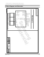
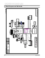
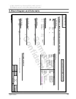
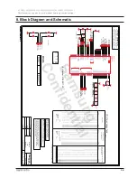
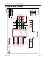
BOARD INFORMATION
SCHEMATIC ANNOTATIONS AND BOARD INFORMATIO
N
See rev notes for more information.
32.768KHz
Crystal
ICH9-M
10MHz
CARD READER(AU6336)
4
5
UHCI_2
BLUETOOTH(TBD)
10
11
Crystal
MICO
M
25MHz
Crystal
LAN
14.318MHz
Crystal
CLOCK-Generator
REVISION HISTORY
I C / SMB Address
ODD
-
SATA2
SATA
3
-
PCI EXPRESS Assignation
Port Numbe
r
Clock, Unused Clock Output Disabl
e
D2
h
CK-505M (Clock Generator)
1101 001X
-
A0h
SODIMM0
-
PCIe3
PCIe
4
-
Crystal / Oscillator
TYP
E
P
REQUENCY
EMC2102
7Ah
0111 101X
A4h
X1
00
0
10
1
1
M
MI
D
O
S
USB PORT Assignatio
n
Port Number
ASSIGNED TO
USB PORT (RIGHT, SUB)
0
5.0V supply for Audi
o
AUD_P5V
PRTC_BAT
3.3V supply for the RTC well
.
Charger Reference Voltage Sourc
e
VDC_CHG
LCD_VDD3V
UHCI_0
UHCI_1
UHCI_3
UHCI_4
Port Number
ASSIGNED TO
CAMERA(17")
P3.3V_MC
D
3.3V (3-in-1 Socket
)
P12.0V_AL
W
12.0V always power well
Power Rail
Descriptions
P5.0V
UHCI_5
USB PORT (LEFT)
USB PORT (RIGHT, SUB)
SATA Assignation
Port Number
ASSIGNED TO
HDD
SATA0
SATA1
Port Number
ASSIGNED TO
1.5V Power Rail (off in S3-S5)
1.05V Power Rail (off in S3-S5)
5.0V Power Rail (off in S4-S5)
3.3V Power Rail (off in S4-S5)
1.5V Power Rail (off in S4-S5)
Core Voltage for CP
U
KBC3_CHG4.2V
ASSIGNED TO
WLAN
PCIe1
PCIe2
Port Number
ASSIGNED TO
Wired LA
N
P1.8_AUX
1.8V Power Rail (off in S4-S5)
P2.0V_VREF
Power Chip Reference
Auido Analog Voltag
e
P4.75V_AUD
To charge USB device at sleep status
E
G
A
S
U
E
CI
V
E
D
Voltage Rail
s
Primary DC system power supply (9 to 19V)
VDC VDC_ADP
T
P3.3V_MICO
M
Power Rail
Descriptions
Output voltage of RT8205AGQ
W
(if VDC is removed, it will be off)
PROPRIETARY INFORMATION THAT IS
A
DO NOT DISCLOSE TO OR DUPLICATE FOR OTHER
S
B
2
C
1
3.3V (LED LCD)
P1.05V_PEG
P1.05V (Direct Media Interface Compensation)
P1.2V_LA
N
Internal Regulator’s Power of LAN Controller
P5.0V_AL
W
5.0V always power well
3
B
RE
V
1
TITLE
C
P3.3V
P1.8V
P1.5V
P1.05
P5.0V_AUX
P3.3V_AUX
P1.5_AUX
CPU_CORE
5.0V Power Rail (off in S3-S5)
3.3V Power Rail (off in S3-S5)
1.8V Power Rail (off in S3-S5)
PAGE
2
SAMSUN
G
D
4
THIS DOCUMENT CONTAINS CONFIDENTIA
L
DRA
W
To charge battery
P0.9V
DDR2 Terminatio
n
P1.7V_VREF
Power Chip Reference
P5.0V_VREF_FILT
Power Chip Reference
DEV. STEP
PART NO
.
ELECTRONICS
OF
CHECK
LAST EDIT
DAT
E
P5.0V_STB
5.0V supply at SUB_ODD Boar
d
P5.0V_ODD
EGFX_COR
E
nVidia Graphic Chip powe
r
2
Power source of External
CAMERA(15")
P2.5V_LA
N
EXCEPT AS AUTHORIZED BY SAMSUNG
.
APPROVAL
Jun PARK
YM.AHN
HJ.KIM
undefined
9/23/2008
PV
1.0
October 27, 2009 14:27:43 PM
BA41-xxxxxA
3
59
Bremen-
L
MAI
N
BOARD INFO
D:/users/mobile24/mentor/Bremen-L/PV/Bremen-L_MAI
N
D
SAMSUNG ELECTRONICS CO’S PROPERTY.
4
SAMSUNG PROPRIETAR
Y
3
A
MODULE CODE
Summary of Contents for R530
Page 5: ...iii Contents This Document can not be used without Samsung s authorization R530 R730...
Page 64: ...6 40 6 Material List This Document can not be used without Samsung s authorization R530 R730...
Page 240: ...4 23 4 Troubleshooting This Document can not be used without Samsung s authorization R530 R730...
Page 241: ...4 24 4 Troubleshooting This Document can not be used without Samsung s authorization R530 R730...
Page 249: ...4 32 4 Troubleshooting This Document can not be used without Samsung s authorization R530 R730...

