background image

2-21

2. Introduction and Specification

- 이 문서는 삼성전자의 기술 자산으로 승인자만이 사용할 수 있습니다 -
- This Document can not be used without Samsung's authorization -

R530/R730

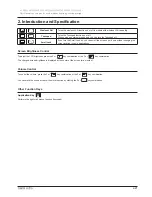
Wireless LAN

Turns the wireless LAN function on or off in models with wireless LAN capability..

Touchpad

Turns the Touchpad function on or off.  

When using an external mouse only, you can turn the Touchpad off.

Scroll Lock

If you turn the Scroll Lock on, you can scroll the screen up or down without changing the 

cursor location in some applications.

Screen Brightness Control

To adjust the LCD brightness press the Fn +  

 key combination or the Fn +  


key combination.

The changed screen brightness is displayed at the center of the screen for a moment.

Volume Control

To control the volume, press the Fn + 


key combination or the Fn + 


key combination.

You can mute the sound or cancel the mute function by clicking the Fn + 

 key combination. 

Other Function Keys

Application Key  

Performs the right-click mouse function (touchpad).

Summary of Contents for R530

Page 1: ...option 2 Convenient functions For Internal Camera Option convenient usage of filming and taking pictures Convenient connection with TV as HDMI port is provided 3 consideration of practical usage Feat...

Page 2: ...tion However succeeding computers and manuals are subject to change without notice Therefore SAMSUNG Electronics Co Ltd assumes no liability for damages incurred directly or indirectly from errors omi...

Page 3: ...tup 2 26 2 9 Mainboard Part Description 2 34 3 Disassembly and Reassembly 3 1 R530 R730 Disassembly and assembly 3 1 4 Troubleshooting 4 1 General 4 1 4 2 Debugging Flow Chart 4 2 4 3 System Diagnosis...

Page 4: ...20 5 19 17 UNIT HOUSING BOTTOM 5 21 5 20 17 UNIT HOUSING BOTTOM LIST 5 22 5 21 17 UNIT HOUSING TOP 1 5 23 5 22 17 UNIT HOUSING TOP 2 5 24 5 23 17 UNIT HOUSING TOP 1 2 LIST 5 25 6 Material List 6 1 15...

Page 5: ...iii Contents This Document can not be used without Samsung s authorization R530 R730...

Page 6: ...nual is a property of Samsung Electronics Co Ltd Any unauthorized use of Manual can be punished under applicable International and or domestic law Samsung Electronics Co Ltd October 2009 Printed in Ko...

Page 7: ...ain System 1 Before disassembling the system the AC adapter and the battery have to be separated 1 1 2 2 As shown in picture 1 Slide the KNOB to the end closely into the arrow direction then push the...

Page 8: ...shown in the picture and then lift the key board up Notice When you push the hook up you have to be careful not to scratch on TOP 6 As shown in the picture lift the top side of keyboard up and then d...

Page 9: ...9 Remove the HDD 1 After removing the screws 2EA for fixing HDD and remove the cover to the arrow direction M2 x L4 Black 2EA 2 With holding the insulator separate the HDD from the connector by pushin...

Page 10: ...authorization R530 R730 Part Picture Description Main System 4 Remove the screws 2 EA for fixing the HDD and separate the HDD from the bracket 10 Remove the memory door 1 Remove the screw 2EA for fixi...

Page 11: ...e screw for fixing ODD M2 x L8 Black 1 EA 2 Separate the ODD from the bottom cover by pushing it to the arrow direction 12 Remove the WLAN cable from the WLAN board 13 Remove the bottom screws M2 x L8...

Page 12: ...iption Main System 15 Remove the speaker cable 16 Condition after removing the T P and speaker cable 17 As shown in the picture separate Front cover by widening the gap between the Front cover and the...

Page 13: ...D ODD and USB board 20 Remove the Main board 1 Remove the screws which fix the Main board and then separate Main board from Bottom M2 x L4 2 EA 21 Conditions of Main board which is separated 1 2 22 Re...

Page 14: ...g the screw for fixing CPU to counterclockwise fully 25 Remove the WLAN board 1 Remove the screw 1EA for fixing the WLAN Board M2 X L3 1ea Black 2 Remove the WLAN Board from the connector 26 Remove th...

Page 15: ...Remove the screw 1 EA for fixing the ODD sub board as shown in the picture M2 X L4 1ea 2 Remove the ODD sub board 29 Remove the USB sub board 1 Remove the screw 2 EA for fixing the USB sub board as sh...

Page 16: ...cause WLAN cable is fixed with the gutter of bottom cover 31 After removing the Rubber LCD cap as shown in the picture remove the screws M2 x L6 6EA Notice Be careful not to make scratch on the LCD Pa...

Page 17: ...e cover part up with your fingers and then separate the bottom side of the LCD 3 Conditions after removing the LCD Cover 33 Remove the LCD panel 1 As shown in the picture remove the screw 6EA which fi...

Page 18: ...removing the LCD panel 34 Remove the screws 6EA for fixing LCD panel and bracket of both sides and remove the LCD brackets as shown in the picture 35 With the LCD panel upside down remove the LCD cab...

Page 19: ...l and shield pad for preventing electromagnetic interference fixed with adhesive on LCD bottom cover 1 Remove the main and aux antenna cable from the LCD Pad 2 Remove the LCD pad and shield pad 38 Rem...

Page 20: ...move the screws 2 EA for fixing the both sides of Hinge as shown in the picture 2 Separate the LCD module and Bottom Cover Notice Carefully remove it because WLAN cable is fixed with the gutter of bot...

Page 21: ...k and LCD front and then separate first the upper part of the LCD front and second both side of the LCD front 2 After lift Hinge cover part up with your fingers and then separate the bottom side of th...

Page 22: ...escription LCD Ass y 17 2 Disassemble the connector from the camera module as shown in the picture 3 Conditions after removing the LCD panel 34 Remove the screws 6EA for fixing LCD panel and bracket o...

Page 23: ...ed with the adhesive tape 37 Remove the LCD pad for preventing shock of LCD panel and shield pad for preventing electromagnetic interference fixed with adhesive on LCD bottom cover 1 Remove the main a...

Page 24: ...3 18 3 Disassembly and Reassembly This Document can not be used without Samsung s authorization R530 R730...

Page 25: ...T54A 30V 200mA SOT 23 TP 3 0505 001088 Q500 1 FET SILICON AO4807L P 30V 6A 0 028 0 035ohm 2W SOIC 8 3 0505 001844 Q501 1 FET SILICON SI4435DDY T1 GE3 P 30V 11 4A 0 024ohm 5W SO 8 3 0505 001883 Q28 1 F...

Page 26: ...05 3 2007 000309 R800 1 R CHIP 10ohm 5 1 10W TP 1608 3 2007 000503 R644 1 R CHIP 2 2ohm 5 1 10W TP 1608 3 2007 000695 R527 1 R CHIP 3 3ohm 5 1 10W TP 1608 3 2007 000695 R548 1 R CHIP 3 3ohm 5 1 10W TP...

Page 27: ...R750 1 R CHIP 56ohm 5 1 16W TP 1005 3 2007 002970 R751 1 R CHIP 56ohm 5 1 16W TP 1005 3 2007 002970 R752 1 R CHIP 56ohm 5 1 16W TP 1005 3 2007 002970 R753 1 R CHIP 56ohm 5 1 16W TP 1005 3 2007 002970...

Page 28: ...007142 R667 1 R CHIP 10Kohm 1 1 16W TP 1005 3 2007 007142 R668 1 R CHIP 10Kohm 1 1 16W TP 1005 3 2007 007142 R670 1 R CHIP 10Kohm 1 1 16W TP 1005 3 2007 007142 R687 1 R CHIP 10Kohm 1 1 16W TP 1005 3 2...

Page 29: ...1 R CHIP 12 1ohm 1 1 16W TP 1005 3 2007 007642 R676 1 R CHIP 12 1ohm 1 1 16W TP 1005 3 2007 007642 R677 1 R CHIP 12 1ohm 1 1 16W TP 1005 3 2007 007766 R509 1 R CHIP 2Kohm 1 1 16W TP 1005 3 2007 00776...

Page 30: ...812 C513 1 C CER CHIP 033nF 5 50V C0G 1005 3 2203 000812 C525 1 C CER CHIP 033nF 5 50V C0G 1005 3 2203 000812 C545 1 C CER CHIP 033nF 5 50V C0G 1005 3 2203 000812 C546 1 C CER CHIP 033nF 5 50V C0G 100...

Page 31: ...HIP 100nF 10 10V X7R TP 1005 3 2203 006048 C600 1 C CER CHIP 100nF 10 10V X7R TP 1005 3 2203 006048 C601 1 C CER CHIP 100nF 10 10V X7R TP 1005 3 2203 006048 C602 1 C CER CHIP 100nF 10 10V X7R TP 1005...

Page 32: ...HIP 100nF 10 10V X7R TP 1005 3 2203 006048 C765 1 C CER CHIP 100nF 10 10V X7R TP 1005 3 2203 006048 C767 1 C CER CHIP 100nF 10 10V X7R TP 1005 3 2203 006048 C769 1 C CER CHIP 100nF 10 10V X7R TP 1005...

Page 33: ...000nF 10 6 3V X5R TP 2012 3 2203 006090 C655 1 C CER CHIP 10000nF 10 6 3V X5R TP 2012 3 2203 006090 C656 1 C CER CHIP 10000nF 10 6 3V X5R TP 2012 3 2203 006090 C667 1 C CER CHIP 10000nF 10 6 3V X5R TP...

Page 34: ...3 2203 006824 C674 1 C CER CHIP 4700nF 10 10V X5R 1608 3 2402 001042 EC500 1 C AL SMD 100uF 20 16V GP TP 6 6x6 6x5 4mm 3 2409 001159 EC502 1 C ORGANIC SMD 220uF 20 2 5V TP 3 5x2 8x1 9mm 3 2603 000099...

Page 35: ...MT SUB MATERIAL RIBBON SOLVENT BOND 4 0201 000160 PART ADHESIVE 0 001 ADHESIVE TS D520 NTR 4 0201 001002 ABLE BOND 0 001 ADHESIVE TS 8380 SIL 9000CPS 10cc 4 0202 001499 0 6 SMT 1 SOLDER WIRE FLUX SR34...

Page 36: ...N 14P 3 5x3 5mm 0 75V to 5 5V 80W 40to 85C 0 75V TP 3 1203 006056 U12 1 IC POSI ADJUST REG APL5930 KAI TRG SOP 8P 4 9x3 9mm PLASTIC 0 8 3 3 3W 40to 85C 3A 0 8 TR 3 1203 006083 U14 1 IC POSI ADJUST REG...

Page 37: ...R CHIP 100Kohm 1 1 16W TP 1005 3 2007 007107 R195 1 R CHIP 100Kohm 1 1 16W TP 1005 3 2007 007107 R198 1 R CHIP 100Kohm 1 1 16W TP 1005 3 2007 007107 R814 1 R CHIP 100Kohm 1 1 16W TP 1005 3 2007 00710...

Page 38: ...7 007318 R144 1 R CHIP 1Kohm 1 1 16W TP 1005 3 2007 007318 R145 1 R CHIP 1Kohm 1 1 16W TP 1005 3 2007 007318 R16 1 R CHIP 1Kohm 1 1 16W TP 1005 3 2007 007318 R43 1 R CHIP 1Kohm 1 1 16W TP 1005 3 2007...

Page 39: ...10 50V X7R TP 1005 3 2203 000438 C129 1 C CER CHIP 1nF 10 50V X7R TP 1005 3 2203 000438 C151 1 C CER CHIP 1nF 10 50V X7R TP 1005 3 2203 000438 C152 1 C CER CHIP 1nF 10 50V X7R TP 1005 3 2203 000438 C1...

Page 40: ...R CHIP 100nF 10 10V X7R TP 1005 3 2203 006048 C170 1 C CER CHIP 100nF 10 10V X7R TP 1005 3 2203 006048 C174 1 C CER CHIP 100nF 10 10V X7R TP 1005 3 2203 006048 C178 1 C CER CHIP 100nF 10 10V X7R TP 10...

Page 41: ...090 C83 1 C CER CHIP 10000nF 10 6 3V X5R TP 2012 3 2203 006090 C844 1 C CER CHIP 10000nF 10 6 3V X5R TP 2012 3 2203 006166 C10 1 C CER CHIP 100nF 10 25V X5R 1005 3 2203 006166 C100 1 C CER CHIP 100nF...

Page 42: ...P 1000nF 10 6 3V X5R 1005 3 2203 006399 C210 1 C CER CHIP 1000nF 10 6 3V X5R 1005 3 2203 006399 C221 1 C CER CHIP 1000nF 10 6 3V X5R 1005 3 2203 006399 C231 1 C CER CHIP 1000nF 10 6 3V X5R 1005 3 2203...

Page 43: ...001649 B6 1 BEAD SMD 180ohm 1608 TP 226ohm 389MHz 3 3301 001649 B7 1 BEAD SMD 180ohm 1608 TP 226ohm 389MHz 3 3301 001649 B8 1 BEAD SMD 180ohm 1608 TP 226ohm 389MHz 3 3301 001649 B9 1 BEAD SMD 180ohm...

Page 44: ...200mA SOT 23 TP 3 0505 001088 Q500 1 FET SILICON AO4807L P 30V 6A 0 028 0 035ohm 2W SOIC 8 3 0505 001844 Q501 1 FET SILICON SI4435DDY T1 GE3 P 30V 11 4A 0 024ohm 5W SO 8 3 0505 001883 Q28 1 FET SILIC...

Page 45: ...m 5 1 16W TP 1005 3 2007 000171 R518 1 R CHIP 0ohm 5 1 16W TP 1005 3 2007 000171 R541 1 R CHIP 0ohm 5 1 16W TP 1005 3 2007 000171 R542 1 R CHIP 0ohm 5 1 16W TP 1005 3 2007 000171 R557 1 R CHIP 0ohm 5...

Page 46: ...3 2007 002970 R708 1 R CHIP 56ohm 5 1 16W TP 1005 3 2007 002970 R709 1 R CHIP 56ohm 5 1 16W TP 1005 3 2007 002970 R710 1 R CHIP 56ohm 5 1 16W TP 1005 3 2007 002970 R711 1 R CHIP 56ohm 5 1 16W TP 1005...

Page 47: ...007142 R559 1 R CHIP 10Kohm 1 1 16W TP 1005 3 2007 007142 R574 1 R CHIP 10Kohm 1 1 16W TP 1005 3 2007 007142 R575 1 R CHIP 10Kohm 1 1 16W TP 1005 3 2007 007142 R576 1 R CHIP 10Kohm 1 1 16W TP 1005 3...

Page 48: ...007 007312 R792 1 R CHIP 20Kohm 1 1 16W TP 1005 3 2007 007318 R511 1 R CHIP 1Kohm 1 1 16W TP 1005 3 2007 007318 R526 1 R CHIP 1Kohm 1 1 16W TP 1005 3 2007 007318 R586 1 R CHIP 1Kohm 1 1 16W TP 1005 3...

Page 49: ...203 000438 C611 1 C CER CHIP 1nF 10 50V X7R TP 1005 3 2203 000438 C622 1 C CER CHIP 1nF 10 50V X7R TP 1005 3 2203 000438 C623 1 C CER CHIP 1nF 10 50V X7R TP 1005 3 2203 000438 C669 1 C CER CHIP 1nF 10...

Page 50: ...X7R TP 1005 3 2203 006048 C524 1 C CER CHIP 100nF 10 10V X7R TP 1005 3 2203 006048 C527 1 C CER CHIP 100nF 10 10V X7R TP 1005 3 2203 006048 C551 1 C CER CHIP 100nF 10 10V X7R TP 1005 3 2203 006048 C55...

Page 51: ...HIP 100nF 10 10V X7R TP 1005 3 2203 006048 C718 1 C CER CHIP 100nF 10 10V X7R TP 1005 3 2203 006048 C719 1 C CER CHIP 100nF 10 10V X7R TP 1005 3 2203 006048 C726 1 C CER CHIP 100nF 10 10V X7R TP 1005...

Page 52: ...6090 C537 1 C CER CHIP 10000nF 10 6 3V X5R TP 2012 3 2203 006090 C538 1 C CER CHIP 10000nF 10 6 3V X5R TP 2012 3 2203 006090 C539 1 C CER CHIP 10000nF 10 6 3V X5R TP 2012 3 2203 006090 C540 1 C CER CH...

Page 53: ...ER CHIP 4700NF 10 25V X5R 2012 3 2203 006377 C715 1 C CER CHIP 4700NF 10 25V X5R 2012 3 2203 006377 C725 1 C CER CHIP 4700NF 10 25V X5R 2012 3 2203 006399 C500 1 C CER CHIP 1000nF 10 6 3V X5R 1005 3 2...

Page 54: ...MODULAR 8P 8C STANDARD N SMD A GRN YEL Au 1PORT 3 3722 002925 J502 1 JACK USB 4P 2C AUF BLK ANGLE OFFSET A 3 3722 002997 J500 1 JACK DC POWER 3P 5 6PI AUF BLK 3 4309 001022 J522 1 BATTERY HOLDER CELL...

Page 55: ...Q517 1 FET SILICON RHU002N06 N 60V 200MA 3 3OHM 0 15W SOT 323 3 0505 001883 Q6 1 FET SILICON RHU002N06 N 60V 200MA 3 3OHM 0 15W SOT 323 3 0505 001883 Q8 1 FET SILICON RHU002N06 N 60V 200MA 3 3OHM 0 1...

Page 56: ...190 1 R CHIP 10ohm 1 1 10W TP 1608 3 2007 002899 R20 1 R CHIP 10ohm 1 1 10W TP 1608 3 2007 002899 R21 1 R CHIP 10ohm 1 1 10W TP 1608 3 2007 002899 R22 1 R CHIP 10ohm 1 1 10W TP 1608 3 2007 002899 R38...

Page 57: ...007142 R97 1 R CHIP 10Kohm 1 1 16W TP 1005 3 2007 007142 R98 1 R CHIP 10Kohm 1 1 16W TP 1005 3 2007 007142 R99 1 R CHIP 10Kohm 1 1 16W TP 1005 3 2007 007239 R151 1 R CHIP 31 6Kohm 1 1 10W TP 1608 3 20...

Page 58: ...R9 1 R CHIP 3 01Kohm 1 1 16W TP 1005 3 2007 008429 R83 1 R CHIP 499ohm 1 1 16W TP 1005 3 2007 008708 R28 1 R CHIP 40 2ohm 1 1 16W TP 1005 3 2007 008708 R29 1 R CHIP 40 2ohm 1 1 16W TP 1005 3 2007 0087...

Page 59: ...203 005509 C837 1 C CER CHIP 330nF 80 20 10V Y5V TP 1005 3 2203 006000 C57 1 C CER CHIP 1nF 10 3000V X7R TP 4520 3 2203 006048 C101 1 C CER CHIP 100nF 10 10V X7R TP 1005 3 2203 006048 C111 1 C CER CHI...

Page 60: ...F 10 6 3V X5R TP 2012 3 2203 006090 C113 1 C CER CHIP 10000nF 10 6 3V X5R TP 2012 3 2203 006090 C114 1 C CER CHIP 10000nF 10 6 3V X5R TP 2012 3 2203 006090 C132 1 C CER CHIP 10000nF 10 6 3V X5R TP 201...

Page 61: ...3 2203 006377 C29 1 C CER CHIP 4700NF 10 25V X5R 2012 3 2203 006377 C37 1 C CER CHIP 4700NF 10 25V X5R 2012 3 2203 006377 C38 1 C CER CHIP 4700NF 10 25V X5R 2012 3 2203 006377 C39 1 C CER CHIP 4700NF...

Page 62: ...EAD SMD 180ohm 1608 TP 226ohm 389MHz 3 3301 001649 B22 1 BEAD SMD 180ohm 1608 TP 226ohm 389MHz 3 3301 001649 B23 1 BEAD SMD 180ohm 1608 TP 226ohm 389MHz 3 3301 001649 B24 1 BEAD SMD 180ohm 1608 TP 226...

Page 63: ...al List This Document can not be used without Samsung s authorization R530 R730 Level Code Assembled EA Description Spec Service 1 BA99 07566A SUB MATERIAL 1 ASSY SUB MATERIAL NP_PBA N P PBA SUB MATER...

Page 64: ...6 40 6 Material List This Document can not be used without Samsung s authorization R530 R730...

Page 65: ...5 EXPLODED VIEW 5 1 This Document can not be used without Samsung s authorization SYSTEM I0005 W3007 G0011 D1002 T0300 M0008 G0003 I0006 T0001 I0009 T2000 B0003 B0701 I0002 M3005 B0001 D0005 M0001...

Page 66: ...5 EXPLODED VIEW 5 2 This Document can not be used without Samsung s authorization ASSY LCD I0013 K0100 K0002 K4001 K0201 I0003 K4002 K3002 K3001 K0001 K2001 K1001 K2002...

Page 67: ...5 EXPODED VIEW 5 3 This Document can not be used without Samsung s authorization UNIT HOSUNG_TOP T2000 T0302 T0001 T0101 T0407...

Page 68: ...5 EXPLODED VIEW 5 4 This Document can not be used without Samsung s authorization UNIT HOSUNG_BOTTOM B0501 B0001 B0302 B0303 B0009 B0009 B0403 B0402 B0010 B0001...

Page 69: ...5 EXPLODED VIEW 5 5 This Document can not be used without Samsung s authorization Unit ODD D3000 D1002 D2000...

Page 70: ...ULTI BREMEN 15L PC A 1 SA BA97 02998D 0001 G0003 BA59 02572A MODULE WLAN AR5B95 WLL6160 D99 ROHS 1 1 SA BA92 06338A 0001 G0003 BA59 02573A MODULE WLAN AR5B95 T77H121 05 1x1 Half 1 SA BA92 06338A 0001...

Page 71: ...L1004 BA68 20039A LABEL PPID_E BLADE PET W50 8 L9mm wh 2 SA BA99 16006A 0001 L1004 BA68 20039A LABEL PPID_E BLADE PET W50 8 L9mm wh 1 SA NP R528 DA03HU 0001 M0001 BA92 06338A ASSY MOTHER BD TOP BREME...

Page 72: ...NECTOR HDMI 19P 2R FEMALE ANGLE Au 1 SA BA92 06338C 0001 M9999 3708 002166 CONNECTOR FPC FFC PIC 25P 1 0mm SMD A AU 1 SA BA92 06338C 0001 M9999 3708 002402 CONNECTOR FPC FFC PIC 6P 1 0mm SMD A SnB 1 S...

Page 73: ...ty SA SNA Parent Part 0001 W3006 BA39 00946A CBF HARNESS USB_SUB BOARD CANNES WIRE 1 SA NP R528 DA03HU 0001 W4002 6001 001413 SCREW MACHINE CH M2 L5 NI PLT SWRCH18A 10 SA BA96 04509A 0001 W4002 6001 0...

Page 74: ...f a defect is found repair or replace it immediately There is a danger of electric shock or fire 5 Make sure that it is properly grounded Check the ground of the wall outlet Electricity leakage may ca...

Page 75: ...en soldering a custom IC 11 Take care to not damage the board when installing or separating an Option Board 12 Take care to not break the printed circuit pattern on the PCB when separate an IC 1 3 Gro...

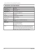
Page 76: ...ore 2 Duo Processor and DDR II Memory option Wireless LAN Improvement for multimedia performance For Internal Camera Option convenient usage of filming and taking pictures Convenient connection with T...

Page 77: ...LCD Viewable Area 382 08 H x 214 92 V 17 3 diagonal LCD Resolution HD 1600 x 900 Win7 Support 1600 X 900 1280 X 768 1280 X 720 1152 X 864 1024 X 768 1024 X 60 800 X 600 XP Support 1600 X 900 1280 X 7...

Page 78: ...M GE1 23x23mm Video Memory 1GB GDDR3 GPU TDP 14W Max Resolution for LFP LVDS dual link resolutionof 1920x1200 per link Max Resolution for External Monitor 2048x1536 at 85Hz Max resolution for VGA MAX...

Page 79: ...Regional Encoding DVD ROM 2 Vendor TEAC DV 28S V Type 12 7 mm S ATA Fixed type Speed 8x DVD ROM 24x CD Average access time DVD 140ms Typ CD 130ms Typ Weight 176g or less Software supplied Cyberlink DV...

Page 80: ...Interface Half Mini card type Chipset Atheros AR5B95 Antenna 2 integrated Feature W30 x L26 8 x H4 75mm Bluetooth N A Type Interface Chipset HSPA N A Ports and interfaces Input output PC card slot 1...

Page 81: ...sor Color CMOS VGA 0 3 Mpixel SCAN mode Progressive Still image capture resolution Max VGA 640 x 480 Video capture resolution Max VGA 640 x 480 Digital video capture speed Max 30 frame USB 2 0 High sp...

Page 82: ...ogram BatteryMark v 4 0 1 Test condition Samsung Optimized LCD Brightness Minimum WLAN R F Off discharged by 3 T4400 2 2GHz DDR2 2GB 15 6 HD LED Intel GL40 250GB DVD Multi Win7 ENG Standard battery 3...

Page 83: ...ion Combo 6cell battery 2 5 250GB HDD with Bundle items Materials PC ABS Vo Installed software Operating system Genuine Windows7 Home Premium Genuine Windows7 Home Basic Genuine Windows Vista Home Bas...

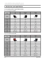
Page 84: ...12MB ATI Radeon HD4650 1GB M961GB M92 512MB GMA4500MHD Shared HDD 250GB 500GB SATA 5400rpm 320GB 500GB SATA 5400rpm 250GB 500GB SATA 5400rpm ODD Super Multi DL Super Multi DL Super Multi DL BR Super M...

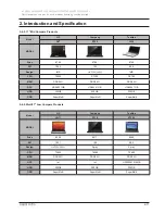
Page 85: ...D RAM 4GB 4GB 4GB HDD 500GB 500GB 400GB ODD Super Multi Super Multi Super Multi BT No BT No BT BT GFX HD4650 1GB HD4650 1GB HD4650 1GB OS Vista Premium Vista Premium Vista Premium 2 4 2 15 6 Compare P...

Page 86: ...R UV IMR CPU T6500 P7350 P8700 MEM DDR2 4G DDR2 4G DDR2 4G GFX HD4650 1GB HD4650 1GB HD4650 1GB HDD 320GB 500GB 320GB ODD SuperMulti SuperMulti SuperMulti 2 4 4 Multi17 Low Compare Products Model HP C...

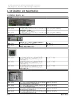
Page 87: ...uetooth 2 1 CPU 0902 002533 CP80617004122AG 2 13GHz PGA988A 988P TR PLASTIC 1 05V 35W 0to 105C 3MB Arrandale i3 330M DDR3 1066 Intel Core i3 330M 0902 002534 CP80617004161AD 2 26GHz PGA988A 988P TR PL...

Page 88: ...5 Inch SATA 5400RPM 250GB P FDB 500GB 5 4KR SATA LCD BA59 02468A N156B6 L06 15 6 Inch HD DE 1366 768 262144 359 3 209 5 450g 3 3V LVDS 6 15 6 LED HD 16 9 Gloss BA59 02505A LTN156AT02 C 15 6 HD LED 220...

Page 89: ...Layer SATA BA96 04533A Purchase BA59 02671A Cuttings TS L633C 8x 190ms SATA 2MB 6 5W 5V Super Multi Dual Layer SATA WLAN BA59 02572A AR5B95 WLL6160 D99 ROHS 1x1 Half MiniCard Standard W308 L26 88 H4 7...

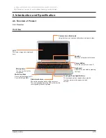
Page 90: ...HC and MMC LCD The screen images are displayed here Touchpad Touchpad Buttons The touchpad and touchpad buttons provide functions similar to the mouse ball and buttons Status Indicators Shows the oper...

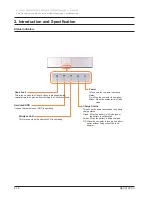
Page 91: ...urce and the battery charge status Green When the battery is fully charged or the battery is not installed Amber When the battery is being charged Off When the computer is running on battery power wit...

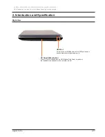
Page 92: ...amsung s authorization R530 R730 Right View USB Port You can connect USB devices to the USB port such as a keyboard mouse digital camera etc CD Drive ODD Option Plays CD or DVD titles Since an ODD Opt...

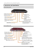
Page 93: ...onnecting the port with a TV v Left View B Type model ExpressCard slot This is a slot which can use ExpressCards A combined port for eSATA and a USB This is a port which can connect a USB device or an...

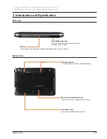
Page 94: ...hargeable battery that supplies power to the computer A ventilating opening It is a place where heat produced by running a computer can be emitted Bottom View Hard disks cover A hard disk is installed...

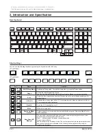
Page 95: ...depending on the keyboard type CRT LCD Switches the screen output to the LCD or external monitor when an external monitor or TV is connected to the computer Backlit Turns the LCD backlight on or off...

Page 96: ...on you can scroll the screen up or down without changing the cursor location in some applications Screen Brightness Control To adjust the LCD brightness press the Fn key combination or the Fn key comb...

Page 97: ...age Manager 8 9 0 1023PV DIPMDisable 8 9 0 1023 Adobe Reader ITA 9 0 0 332 Easy Battery Manager 3 3 2 1 9 Easy SpeedUp Manager 2 0 2 9 Vista 32 64 Marvell LAN Driver 10 100 GbE 11 22 3 3 Media Center...

Page 98: ...1 32bit RUS Language Pack SP1 Vista SP1 32bit ITA Language Pack SP1 Vista SP1 32bit POL Language Pack Vista SP1 32bit DUT Language Pack SP1 Vista SP1 32bit CHS Language Pack SP1 Vista SP1 32bit CHT La...

Page 99: ...bit OptionUpdate Marker File Vista Win7 2 MSetup Patch for Selectable HDM 1 0 0 8 Game Console KOR 1 2 AnyPC 1 0 0 19A Windows Live Wave 3 QFE2 ENG 3 5 MS Office 2007 ready DAN Selectable 1 9 MS Offic...

Page 100: ...E2 DAN 3 5 Windows Live Wave 3 QFE2 FIN 3 5 Windows Live Wave 3 QFE2 NOR 3 5 Windows Live Wave 3 QFE2 SWE 3 5 Recovery Environment 4 4 0 0 4 15GB Recovery Settings 4 4 0 0 31 SW Media Installer for SR...

Page 101: ...emory size 256 MB Shared Selected 256 MB graphics memory size Max Shared Selected maximum graphics memory size Graphics memory in the system of Windows Vista installed will be optimized by DVMT5 0 BIO...

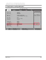
Page 102: ...Shift Tap or Enter selects field SATA Port 1 SAMSUNG HM320II PM SATA Port 2 TSSTcorp CDDVDW TS L633A PM CPU Vendor Intel CPU Speed Core 2 Duo T6600 CPU Speed 2 20 GHz Total Memory 4096MB Slot1 Memory...

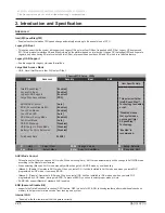
Page 103: ...de Control Auto EDB Execute Disable Bit Enabled Touch Pad Mouse Enabled Touch Pad LED Auto CPU Power Saving Mode Enabled Fan Silent Mode Auto USB S3 Wake up Disabled USB Charge In Sleep Mode Disabled...

Page 104: ...lways Off means that LED always turns off CPU Power Saving Mode Enabled will decrease system power consumption Fan Silent Mode Low will allow the Fan to toggle On Off and regulate the RPM according to...

Page 105: ...assword controls access to system boot Fixed Disk Boot Sector Write Protect will protect to write in Boot Sector of HDD PhoenixBIOS Setup Utility Main Advanced Security Boot Exit Item Specific Help Su...

Page 106: ...f AC adapter at each bootup User Control The brightness values could be remained regardless of the status of AC adapter Wireless Device Control Always On Off The wireless devices are turned on or not...

Page 107: ...5 moves the device up or down x exclude or include the device to boot Shift 1 enables or disables a device 1 4 Loads default boot sequence 1 IDE CD P1 TSSTcorp CDDVDW TS L633A 2 IDE HDD P0 SAMSUNG HM3...

Page 108: ...default values for all SETUP items Discard Changes Load previous values from CMOS for all SETUP items Save Changes Save Setup Data to CMOS PhoenixBIOS Setup Utility Main Advanced Security Boot Exit I...

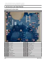
Page 109: ...2 1 DC IN connector 12 Touch PAD Tact S W 2 2 LCD connector 13 ODD connector 3 RGB connector 14 Touchpad connector 4 Lan connector 15 Keyboard connector 5 HDMI connector 16 USB Sub Board Conn 6 USB po...

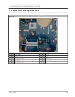
Page 110: ...tion This Document can not be used without Samsung s authorization R530 R730 BOTTOM 6 2 4 5 3 1 7 8 9 1 CPU socket 6 MCH 2 WLAN connector 7 ICH 3 SODIMM connector 8 3 in 1 socket 4 SODIMM connector 9...

Page 111: ...2 36 2 Introduction and Specification This Document can not be used without Samsung s authorization R530 R730...

Page 112: ...D Design CHECK PART NO Model Name Bremen L PBA Name TITLE PCB Code T R Date Revision Dev Step PV 2 Bremen L MAIN 2009 10 27 Remarks Intel Penryn DO NOT DISCLOSE TO OR DUPLICATE FOR OTHERS Montevina P...

Page 113: ...tiga PM45 LVDS 15 Single 17 Dual DDR2 SODIMM x 2 17 3 HD 15 6 LED LCD Page 36 Page 12 Page 20 24 P 2 P 9 15 Single USB Port Dual USB Port UL PAGE B MODULE CODE LAST EDIT PART NO Half Type L R Page 39...

Page 114: ...ower Rail off in S3 S5 5 0V Power Rail off in S4 S5 3 3V Power Rail off in S4 S5 1 5V Power Rail off in S4 S5 Core Voltage for CPU KBC3_CHG4 2V ASSIGNED TO WLAN PCIe1 PCIe2 Port Number ASSIGNED TO Wir...

Page 115: ...POWER DIAGRAM KBC3_VRON VDC KBC3_SUSPWR KBC3_PWRON P5 0V OF EXCEPT AS AUTHORIZED BY SAMSUNG LAST EDIT TITLE PART NO A B D PAGE A 4 SAMSUNG 1 CHECK B MODULE CODE AC ADAPTER P3 3V_MICOM DC BATTERY S5 S...

Page 116: ...AUX 11 CHP3_SLPS5 4 3 16 15 8 14 1 11 17 P3 3V EMC21112 Sheet 45 LED Sheet 47 16 P3 3V 9 P3 3V_AUX 4 P3 3V_MICOM P1 8V AO6409L 10 P1 8V_AUX EGFX_CORE SC471 EGFX_CORE 2 VDC GCORE3_PWRGD APW7141 PRTC_BA...

Page 117: ...CLK0_HCLK1 HCLK1 CLK1_DREFSSCCLK DREFSSCCLK L L P G 3 H C M L L P G 3 H C M _ 1 K L C 4 C R S z H M 0 0 1 AUD3_BCLK CPU MCH KBC 14 318 MHz CK 505M w CLKREQ SSDC FS 2 0 CPU_STP ITP_EN SS 96 100 SEL PC...

Page 118: ...ENTIAL INTEL TR MODE PAGE DEV STEP REV BA61 01090A M505 October 27 2009 14 27 43 PM BA41 xxxxxA 7 59 Bremen L THERMAL SENSOR BA61 01090A M503 LENGTH HEAD DIA LENGTH HEAD DIA 31 C3 44 C3 1 R567 49 9 7...

Page 119: ...22 D1 F24 D10 J24 D11 J23 D12 H22 D13 F26 D14 K22 D15 H23 D16 N22 D17 K25 D18 P26 A3 STPCLK D5 TRDY G2 0143854500 bga_479p_sock CPU1 2 PENRYN LOCK H4 K3 REQ0 H2 REQ1 K2 REQ2 J3 REQ3 L1 REQ4 RESET C1 R...

Page 120: ...Voltage divider within 0 5 0 0 0 1 0 1 0 SAMSUNG PROPRIETARY 0 1 0 1 1 0 0 0 8000 V 0 0 7750 V 0 0 1 1 0 7375 V 0 0 1 1 0 1 1 Active Deeper Sleep 1 1 1 1250 V PART NO 0 0 0 0 1 1 0 1 1 1 0 COMP0 2 COM...

Page 121: ...SS_29 A16 VSS_3 AC19 VSS_30 AC21 VSS_31 AC24 VSS_32 AC3 Y24 VSS_161 Y3 VSS_162 Y6 VSS_163 AA5 VSS_17 AA8 VSS_18 AB1 VSS_19 A14 VSS_2 AB11 VSS_20 AB13 VSS_21 AB16 VSS_22 AB19 VSS_23 VSS_151 V2 VSS_152...

Page 122: ...R692 19 C4 40 C4 34 A4 475 R701 1 R103 42 C3 10V 100nF C152 33 1 6 3V C834 10000nF X5R 31 B4 17 B4 18 B4 nostuff 50V C134 0 022nF 12 B1 P3 3V R693 22 50V C122 0 018nF 1 R699 10K 10000nF X5R C877 100n...

Page 123: ...AH25 VCC_21 AH28 VCC_22 AJ23 VCC_23 AJ26 VCC_24 AJ33 F12 H_RS _1 C8 H_RS _2 H_SWING C5 C9 H_TRDY VCC_1 AA28 VCC_10 AE33 VCC_11 AF23 VCC_12 AF25 VCC_13 AF28 AF33 VCC_14 AG24 H_DVREF B11 H9 H_HIT E12 H...

Page 124: ...43 PEG_RX_7 T42 U42 PEG_RX_8 PEG_RX_9 Y42 PEG_TX _0 J41 PEG_TX _1 M46 PEG_TX _10 Y40 T43 PEG_RX _8 U43 PEG_RX _9 Y43 H43 PEG_RX_0 PEG_RX_1 J44 PEG_RX_10 W47 PEG_RX_11 Y37 PEG_RX_12 AA42 PEG_RX_13 AD36...

Page 125: ...BE45 SB_DQ_21 BC41 SB_DQ_22 BF40 SB_DQ_23 BF41 SB_DQ_24 BG38 BH9 SB_DQS_5 BB2 SB_DQS_6 AU1 SB_DQS_7 AN6 SB_DQ_0 AK47 SB_DQ_1 AH46 SB_DQ_10 BA48 SB_DQ_11 AY48 SB_DQ_12 AT47 SB_DQ_13 AR47 SB_DQ_14 BA47...

Page 126: ...7 VCC_TX_LVDS VSS_AXG_SENSE AH14 VCC_SM_8 AT32 VCC_SM_9 VCC_SM_CK_1 BF20 BF21 VCC_SM_CK_2 BG20 VCC_SM_CK_3 BH20 VCC_SM_CK_4 AM10 VCC_SM_LF_1 AM40 VCC_SM_LF_2 AV21 VCC_SM_LF_3 AV44 VCC_SM_LF_4 AY5 VCC_...

Page 127: ...M6 VSS_296 N11 VSS_297 N13 VSS_298 N16 VSS_299 A18 VSS_3 AD38 VSS_30 N20 VSS_300 N25 VSS_301 VSS_283 L36 VSS_284 L39 VSS_285 L42 VSS_286 L47 VSS_287 L5 VSS_288 L8 VSS_289 AD2 VSS_29 M10 VSS_290 M17 V...

Page 128: ...113 CAS CK0 30 32 CK0 164 CK1 166 CK1 79 CKE0 80 CKE1 10 DDR2M2 1 DDR2 SODIMM 200P STD 3709 001573 sodimm 200p s 4 1 102 A0 101 A1 105 A10_AP 90 A11 89 A12 A13 116 86 A14 84 A15 85 A16_BA2 100 A2 99...

Page 129: ...SODIMM 200P RVS DDR2M1 2 GND0 2 14 C1 18 C4 27 22 51 B1 14 D1 17 C3 14 D1 18 C4 18 19 20 P1 8V_AUX 48 16 14 C1 13 C922 100nF 10V 100nF C919 12 31 B4 6 43 10V 42 10V 2200nF X5R C923 11 B4 17 B4 35 14...

Page 130: ...PEX_RX0 AP17 AN17 AK20 PEX_IOVDDQ_22 AK23 PEX_IOVDDQ_23 AK26 PEX_IOVDDQ_24 PEX_IOVDDQ_25 AL16 PEX_IOVDDQ_3 AG13 PEX_IOVDDQ_4 AG15 AG16 PEX_IOVDDQ_5 AG17 PEX_IOVDDQ_6 PEX_IOVDDQ_7 AG18 PEX_IOVDDQ_8 AG2...

Page 131: ...2 B25 FBC_D63 A25 G19 FBC_DEBUG FBC_DQM0 A16 FBC_DQM1 D10 F11 FBC_DQM2 FBC_DQM3 D15 FBC_DQM4 FBC_D48 B29 FBC_D49 C31 FBC_D50 C29 FBC_D51 B31 FBC_D52 C32 B32 FBC_D53 FBC_D54 B35 FBC_D55 B34 A29 FBC_D56...

Page 132: ...VDD_19 L12 VDD_2 VDD_100 AC21 VDD_101 AC22 VDD_102 AC23 VDD_103 AC24 VDD_104 AC25 VDD_105 AD12 VDD_106 AD14 VDD_107 AD16 VDD_108 AD18 VDD_109 L21 VDD_11 AD22 V2 GND_92 V5 GND_93 V9 GND_94 V12 GND_95 V...

Page 133: ...AM6 IFPC_L1 AL5 IFPC_L1_N AM5 IFPC_L2 AM3 IFPC_L2_N AM4 IFPC_L3 AP1 IFPC_L3_N AG10 IFPB_TXC AP13 IFPB_TXC_N AN13 IFPB_TXD4 AN8 IFPB_TXD4_N AP8 IFPB_TXD5 AP10 IFPB_TXD5_N AN10 IFPB_TXD6 AR11 IFPB_TXD6...

Page 134: ...MIOA_DE N3 MIOA_HSYNC P9 MIOA_VDDQ_1 R9 R4 MIOA_CLKOUT T4 MIOA_CLKOUT_N P5 MIOA_CTL3 N1 MIOA_D0 P4 MIOA_D1 U2 MIOA_D10 U3 MIOA_D11 R6 MIOA_D12 T6 MIOA_D13 N6 MIOA_D14 P1 DACB_RSET AG7 DACB_VDD AK6 DA...

Page 135: ...NC_CS1 J1 NC_ODT1 L9 NC_ZQ1 F2 DQL3 F8 DQL4 H3 DQL5 H8 DQL6 G2 H7 DQL7 DQSL F3 DQSL G3 DQSU C7 B7 DQSU DQU0 D7 DQU1 BA2 M3 CAS K3 CK J7 CK K7 K9 CKE_CKE0 L2 CS _CS0 DML E7 DMU D3 DQL0 E3 DQL1 F7 DQL2...

Page 136: ...T A1 VDDQ_1 A8 VDDQ_2 C1 VDDQ_3 C9 VDDQ_4 D2 VDDQ_5 E9 VDDQ_6 F1 VDDQ_7 H2 VDDQ_8 DQU1 C8 DQU2 C2 DQU3 A7 DQU4 A2 DQU5 B8 DQU6 A3 DQU7 J9 NC_CE1 L1 NC_CS1 J1 NC_ODT1 L9 NC_ZQ1 K1 F8 DQL3 H3 DQL4 H8 DQ...

Page 137: ...U4 DQU5 A2 B8 DQU6 A3 DQU7 J9 NC_CE1 L1 NC_CS1 J1 NC_ODT1 DQL1 F2 DQL2 F8 DQL3 H3 DQL4 H8 DQL5 DQL6 G2 H7 DQL7 F3 DQSL G3 DQSL C7 DQSU B7 DQSU D7 N8 BA1 M3 BA2 K3 CAS J7 CK K7 CK K9 CKE_CKE0 L2 CS _CS...

Page 138: ..._8 G1 VSSQ_9 G9 VSS_1 A9 VSS_10 P9 VSS_11 T1 VSS_12 T9 VSS_2 B3 VSS_3 E1 VSS_4 N1 VDD_7 N9 VDD_8 R1 VDD_9 R9 VREFCA M8 VREFDQ H1 VSSQ_1 B1 VSSQ_2 B9 VSSQ_3 D1 VSSQ_4 D8 VSSQ_5 E2 C9 VDDQ_5 D2 VDDQ_6 E...

Page 139: ...PPROVAL MODULE CODE DATE DEV STEP 0001 35K 0011 0110 SAMSUNG PROPRIETARY 1011 PROPRIETARY INFORMATION THAT IS PCI_DEVID 1 ELECTRONICS A A N11x series PCIE swing level N11M GE1 15K PU ROM_SCLK N11M GE1...

Page 140: ...N AG17 SATA0TXP AH13 SATA1RXN AJ13 SATA1RXP AG14 SATA1TXN AF14 SATA1TXP SATA4RXN AH11 SATA4RXP AJ11 SATA4TXN AG12 SATA4TXP AF12 SATA5RXN E13 LAN_TXD2 LDRQ0 J3 LDRQ1 _GPIO23 J1 AF23 NMI PECI AG27 RCIN...

Page 141: ..._GPIO52 F13 REQ3 _GPIO54 E6 SERR J4 SPI_CLK M26 PETP2 PETP3 K26 H26 PETP4 PETP5 F26 PETP6_GLAN_TXP D26 PIRQA J5 PIRQB E1 PIRQC J6 PIRQD C4 PIRQE _GPIO2 H4 PIRQF _GPIO3 K6 PERP4 PERP5 E28 PERP6_GLAN_RX...

Page 142: ...C16 SLP_S3 E16 SLP_S4 G17 SLP_S5 A17 SMALERT _GPIO11 G16 SMBCLK SMBDATA A13 SMLINK0 C17 D19 F19 RI D22 RSMRST C10 S4_STATE _GPIO26 SATA0GP_GPIO21 AH23 AF19 SATA1GP_GPIO19 AE21 SATA4GP_GPIO36 AD20 SAT...

Page 143: ...9 F9 G3 VCC3_3_10 T29 VCC1_5_B_39 U24 VCC1_5_B_40 U25 VCC1_5_B_41 V24 VCC1_5_B_42 V25 VCC1_5_B_43 U23 VCC1_5_B_44 W24 VCC1_5_B_45 W25 VCC1_5_B_46 VCC1_5_B_47 K23 VCC1_5_B_48 Y24 VCC1_5_B_49 N24 VCC1_5...

Page 144: ...SS_148 P28 VSS_149 P29 VSS_150 P4 VSS_130 N11 VSS_131 N12 VSS_132 N13 VSS_133 N14 VSS_134 N15 VSS_135 N16 VSS_136 N17 VSS_137 N18 VSS_138 N26 VSS_139 N27 VSS_140 VSS_119 L5 VSS_120 L7 VSS_121 M12 VSS_...

Page 145: ...KEYBOARD EERROR 04 GET CPU TYPE 20 TEST DRAM REFRESH 13 PCI BUS MASTER RESET 92 JUMP TO USER PATCH 2 56 ENABLE KEYBOARD 1A 8237 DMA CONTROLLER INIT C0 TRY BOOT WITH INT19 9C SETUP POWER MANAGEMENT C...

Page 146: ...6 27 28 29 3 30 4 5 6 7 8 1 10 11 12 13 14 15 16 17 18 19 2 20 21 25V 19 D1 SOCK 30P 2R SMD MNT J508 3710 002498 P3 3V_AUX VDD_LED C539 4700nF X5R R28 1 100K R14 2 2K P3 3V P5 0V_STB BREMEN15 0 R540 R...

Page 147: ...3V D2 1 3 Q1 RHU002N06 MMBD4148 150 1 P3 3V VCC_CRT VCC_CRT P3 3V R19 PGB1010603NR D504 nostuff 2 1 VCC_CRT 0 022nF C22 23 D1 50V 1 150 R17 1 L6 82nH D505 PGB1010603NR nostuff 2 100nF C530 10V C524 50...

Page 148: ...S 60V Q508 RHU002N06 R634 2 2K P3 3V 37 C2 60V P3 3V 22 B2 P3 3V P3 3V 2 2K R635 100nF C631 10V 37 C2 BLM18PG181SN1 B508 BAV99LT1 D508 1 3 2 D509 BAV99LT1 70V 1 3 2 nostuff 70V R65 47K 1 P3 3V nostuff...

Page 149: ...7 EAPD_SPDIF02 47 GPIO0_DMIC_DATA 3 9V 1205 003769 ALC269Q GR U13 AVDD1 25 38 AVDD2 26 AVSS1 AVSS2 0 1005 R168 5 6 MNT2 P4 75V_AUD P4 75V_AUD B517 BLM18PG181SN1 38 B2 3711 000922 J517 HDR 4P SMD 1 2...

Page 150: ...NICS SAMSUNG THIS DOCUMENT CONTAINS CONFIDENTIAL PAGE DEV STEP B B C G1 G2 B16 BLM18PG181SN1 Jun PARK JACK PHONE 6P BLACK J521 3722 002588 1 2 3 4 5 6 38 C1 BLM18PG181SN1 B17 10nF 25V 38 C1 0 1nF C199...

Page 151: ...1 2 RD RDCT 3 RX 16 15 RX RXCT 1 1K R40 C572 100nF 10V P1 2V_LAN C579 10V 100nF 10V 100nF C69 P3 3V_AUX P3 3V C74 100nF 10V 25MHz Y1 1 2 1 R47 2K C70 100nF 10V 10V C616 4700nF X5R 4700nF X5R C64 10V 1...

Page 152: ...50V 1 33 R238 41 C2 41 C2 330 R232 41 C2 41 C2 470nF C258 16V 10V R242 C235 4700nF X5R 1 11 C4 1 100K 6 3V 1000nF X5R C233 R208 150K 10V C236 100nF P3 3V_MCD 100nF C241 10V 41 C2 P3 3V 31 B1 31 B1 VS3...

Page 153: ...9 14 27 43 PM BA41 xxxxxA 42 59 C72 100nF 11 B1 44 B3 30 B4 100nF C689 R55 10K 1 44 C3 31 C4 40 D4 11 B1 P3 3V 30 C1 34 A4 R613 100 1 12 SIM_DATAIO_C7 10 SIM_RESET_C2 14 SIM_RSVD_C4 19 SIM_RSVD_C8 17...

Page 154: ...ODD SUB CONNECTOR SATA_DEVICES Bremen L 59 43 BA41 xxxxxA October 27 2009 14 27 43 PM 1 0 PV 9 23 2008 HJ KIM YM AHN Jun PARK DEV STEP REV APPROVAL C 1 ELECTRONICS MODULE CODE TITLE 29 B3 29 B3 29 B3...

Page 155: ...ATAOUT_GPIO45 127 IMCLK 35 IMDAT 36 KCLK 61 62 KDAT KSI0 29 28 KSI1 KSI2 99 GPIO31_BC_INT 100 GPIO32 126 GPIO33 65 GPIO34 64 GPIO35 63 GPIO36 1 34 GPIO37_CIR_LED GPIO38_CIR_IN 33 30 GPIO39 HSTCLK_GPIO...

Page 156: ...01 19 217 T3D AER1R2B5Y LED513 1 2 19 217 T3D AER1R2B5Y LED509 BREMEN15 1 2 R610 10K nostuff 1 BREMEN17 1 2 BREMEN17 19 217 T3D AER1R2B5Y LED530 1 2 19 217 T3D AER1R2B5Y LED531 BREMEN17 1 2 LED532 19...

Page 157: ...OF A SAMSUNG Jun PARK YM AHN HJ KIM 9 23 2008 PV 1 0 October 27 2009 14 27 43 PM BA41 xxxxxA 46 59 Bremen L LED_SWITCH LED_SWITCH D users mobile24 mentor Bremen L PV Bremen L_MAIN LEDs LAST EDIT TITLE...

Page 158: ...STEP DESIGN OF PROPRIETARY INFORMATION THAT IS THIS DOCUMENT CONTAINS CONFIDENTIAL MODULE CODE REV B SAMSUNG 100nF C528 10V P3 3V GND MNT1 5 6 MNT2 MNT3 7 8 MNT4 PWR 31 B1 31 B1 31 B1 J520 3722 00276...

Page 159: ...ber 27 2009 14 27 43 PM 1 0 PV 9 23 2008 HJ KIM YM AHN Jun PARK SAMSUNG TITLE A 3 D C 2 B 1 CAMERA 4 2 1 3 SAMSUNG PROPRIETARY EXCEPT AS AUTHORIZED BY SAMSUNG 4 DO NOT DISCLOSE TO OR DUPLICATE FOR OTH...

Page 160: ...nostuff G_CHG nostuff C61 16V 470nF 4700nF X5R C510 25V 49 A2 49 B1 50V C60 0 1nF C516 100nF G_CHG G_CHG R49 51 1K nostuff 25V 1 1 43 2K R573 3722 002997 J501 JACK DC POWER 3P MNT GND_1 2 GND_2 3 4 MN...

Page 161: ...X5R 6 3V EC14 330uF 6 3V 15mohm CAN 6T G_P3 3V REF SKIPSEL 14 TONSEL 4 21 UGATE1 10 UGATE2 VIN 16 24 VOUT1 7 VOUT2 VREG3 8 VREG5 17 2409 001175 2 FB1 5 FB2 19 LGATE1 12 LGATE2 18 NC 25 PAD PGND 15 PGO...

Page 162: ...V C257 100nF nostuff C268 1nF 50V SHORT507 INSTPAR G_DDR RHU002N06 Q31 D 3 1 G 2 S 1 10 R245 P1 8V_AUX 60V C256 4700nF X5R 25V P0 9V G_DDR G_DDR RHU002N06 Q33 D 3 1 G 2 S VDC G_DDR 60V 1 R264 17 4K 1...

Page 163: ...239 55 B2 52 C4 53 C4 47nF C254 50V 22K R237 1 G_P1 5V G_P1 5V 100nF C250 25V G_P1 5V G_P1 5V 50V 0 1nF C1002 2 2 R810 7 6V 5 D1 D2 6 G 4 S 3 20K R866 1 7 6V 7 D1 D2 8 G 2 S 1 Q26 2 AP4232BGM HF 0505...

Page 164: ...D3 7 8 D4 4 G 1 S1 S2 2 3 S3 7 8 D4 4 G 1 S1 S2 2 3 S3 Q15 AP6680AGM 30V Q14 AP6680AGM 30V D1 5 6 D2 D3 EC105 330uF 2 5V 2409 001176 100nF C160 19 D1 1 10V P3 3V 20K R134 25V C162 22nF R123 2 2K nost...

Page 165: ...0 39uH EC5 68uF 25V AL 2402 001144 R11 10 1 470 R532 C20 1nF 50V 100nF C28 25V 0 39uH L1 MPO104 R39 2703 002992 50V 0 033nF C556 0 1005 R562 2402 001144 AL 25V 68uF EC4 1 nostuff P1 7V_VREF P1 7V_VRE...

Page 166: ...AO6409L 20V AO6409L Q25 1 D1 D2 2 SHORT9 INSTPAR C276 10V 100nF P5 0V_AUX P5 0V_ALW 60V D 3 1 G 2 S C262 10V 100nF 50V RHU002N06 Q38 0 R879 C234 47nF nostuff 1 nostuff C1018 100nF 10V 100K R882 52 A4...

Page 167: ...s mobile24 mentor Bremen L PV Bremen L_MAIN DISCHARGING LOGIC PWR_MV_DISCHARGER Bremen L 59 56 BA41 xxxxxA October 27 2009 14 27 43 PM 1 0 PV 9 23 2008 undefined nostuff Q39 RHU002N06 nostuff Q24 RHU0...

Page 168: ...rom ME recommedation Jun PARK YM AHN HJ KIM 8 22 2009 PV 1 0 October 27 2009 14 27 43 PM BA41 xxxxxA 57 59 Bremen L SUB BOARD1 USB PORT POWER SW SUBBOARD 57 C4 0 033nF C504 50V PWR0 PWR1 5 USB0 3 2 US...

Page 169: ...SUB BOARD SUB BOARD2 Bremen L 59 58 BA41 xxxxxA October 27 2009 14 27 43 PM 1 0 PV 9 23 2008 undefined HJ KIM YM AHN Jun PARK ODD sub board mount hole Type angle 2 10V C511 100nF G_ODD MNT1 MNT2 14 15...

Page 170: ...09 09 10 Add for EMC 2009 09 10 SAMSUNG DEV STEP 3 A B APPROVAL D 4 100nF C282 25V 100nF C55 P3 3V_LED 25V P3 3V_LED 25V C1039 100nF P1 5V VDC RMNT 30 90 1P MT508 VDC P3 3V 1nF C97 MT519 RMNT 25 70 1P...

Page 171: ...ENTIAL 1 NAN BA41 01178A CHECK SAMSUNG PROPRIETARY MODULE CODE SAMSUNG ELECTRONICS CO S PROPERTY Owner C PART NO CHECK EXCEPT AS AUTHORIZED BY SAMSUNG 4 A PAGE 2 Dev Step PV C REV CPU MAIN 4 3 2009 10...

Page 172: ...CBGA LPC C PG 30 Aud PG 36 USB 8 Circuit OF Channel B Reverse OPTION DDR II CHECK DC DC A DC DC PG 8 2P USB 5 DO NOT DISCLOSE TO OR DUPLICATE FOR OTHERS PG 19 2 IN 1 PG 40 80 Port PG 41 2 HP Mini Card...

Page 173: ...ermal Sensor on SODIMM0 3 0011 000x 2 0011 010x 1 34h Devices Core Voltage for CPU THIS DOCUMENT CONTAINS CONFIDENTIAL VDC Hub to PCI 5 0V always power rail C 0 9V power rail for DDR off in S3 S5 D P5...

Page 174: ...W MODULE CODE S5 S4 Rev 0 1 KBC3_VRON D KBC3_PWRON P0 9V 2 PCMCIA P0 9V ELECTRONICS Battery DC VDC A CRESTLINE It should be updated DRAW ICH8 M ICH8 M EGFX_CORE LEDs P3 3V OPTION FOR ME P2 5V_LAN ICH9...

Page 175: ...ctober 05 2009 20 00 56 PM BA41 xxxxxA 8 50 Bremen UL THERMAL SENSOR THERMAL SENSOR EMC2112 D users mobile29 mentor Bremen UL Bremen UL_Etc TW Kim HJ Kim SJ Park 9 23 2008 ADV2nd 1 0 EXT DIODE 2 MODE...

Page 176: ...D51 AB21 D52 AC26 D53 AD20 D54 AE22 D55 AF23 D56 AC25 D57 AE21 D58 D39 F23 D4 Y25 D40 W22 D41 Y23 D42 W24 D43 W25 D44 AA23 D45 AA24 D46 AB25 D47 AE24 D48 G22 D3 T25 D30 N25 D31 Y22 D32 AB24 D33 V24 D...

Page 177: ...3 1 1 0 1 1 0 0 1 1 1 1 0 0 0 1 3250 V 0 0 0 7625 V 0 7000 V 0 0 0 1 0 9875 V 0 1 0 1 0 1 0 Voltage 0 1 1 1 0 0 1 0 8000 V 0 B 1 0 0 1 0 0 1 1 1500 V 0 1 0 0 1 0125 V 1 1000 V 1 1 4375 V 1 0 1 1 1 1...

Page 178: ...VSS_21 AB16 VSS_22 AB19 VSS_23 AB26 VSS_24 AB4 VSS_25 AB8 VSS_26 AC11 VSS_27 AC14 VSS_28 AC16 VSS_29 A16 VSS_3 W4 VSS_159 AA25 VSS_16 Y21 VSS_160 Y24 VSS_161 Y3 VSS_162 Y6 VSS_163 AA5 VSS_17 AA8 VSS_1...

Page 179: ...S_IO 22 VSS_PCI 15 VSS_PLL3 26 VSS_REF 1 VSS_SRC1 30 36 VSS_SRC2 VSS_SRC3 49 XTAL_IN 3 2 XTAL_OUT 56 VDD_IO 19 VDD_PCI 9 VDD_PLL3 23 27 VDD_PLL3_IO VDD_REF 4 VDD_SRC 46 VDD_SRC_IO1 33 VDD_SRC_IO2 43 V...

Page 180: ...CC_28 U33 VCC_29 VCC_3 AA34 U34 VCC_30 V33 VCC_31 V34 VCC_32 W33 VCC_33 Y33 VCC_34 Y34 AG25 VCC_16 AG26 VCC_17 AG33 VCC_18 AG34 VCC_19 VCC_2 AA33 AH23 VCC_20 AH25 VCC_21 AH28 VCC_22 AJ23 VCC_23 AJ26 V...

Page 181: ...PEG_TX_7 T39 U36 PEG_TX_8 PEG_TX_9 U39 PM_DPRSTP B7 N33 PM_EXT_TS _0 PM_EXT_TS _1 P32 T40 PEG_TX _8 U37 PEG_TX _9 U40 J42 PEG_TX_0 PEG_TX_1 L46 PEG_TX_10 Y39 Y46 PEG_TX_11 PEG_TX_12 AA36 PEG_TX_13 AA...

Page 182: ...36 SB_CKE_1 AV24 SB_CK_0 AU20 SB_CK_1 AV16 SB_CS _0 AR13 SB_CS _1 AM47 SB_DM_0 AY47 SB_DM_1 BD40 SB_DM_2 BF35 SB_DM_3 BG11 SB_DM_4 BA3 SB_DM_5 SA_ODT_0 AY17 SA_ODT_1 BB20 SA_RAS AY20 SA_WE BC16 SB_BS_...

Page 183: ...DS K47 AH14 VSS_AXG_SENSE VCC_SM_9 AT32 BF20 VCC_SM_CK_1 VCC_SM_CK_2 BF21 VCC_SM_CK_3 BG20 VCC_SM_CK_4 BH20 VCC_SM_LF_1 AM10 VCC_SM_LF_2 AM40 VCC_SM_LF_3 AV21 VCC_SM_LF_4 AV44 VCC_SM_LF_5 AY5 VCC_SM_L...

Page 184: ...M41 VSS_295 M44 VSS_296 M6 VSS_297 N11 VSS_298 N13 VSS_299 N16 VSS_3 A18 VSS_30 AD38 VSS_300 N20 VSS_283 L33 VSS_284 L36 VSS_285 L39 VSS_286 L42 VSS_287 L47 VSS_288 L5 VSS_289 L8 VSS_29 AD2 VSS_290 M1...

Page 185: ...62 DQ28 64 DQ29 19 DQ3 74 DQ30 76 DQ31 123 DQ32 125 DQ33 135 DQ34 137 DQ35 124 DQ36 126 DQ37 134 DQ38 7 DQ1 DQ10 35 37 DQ11 20 DQ12 22 DQ13 36 DQ14 38 DQ15 43 DQ16 45 DQ17 55 DQ18 57 DQ19 17 DQ2 44 DQ...

Page 186: ...57 DQ2 17 DQ20 44 DQ21 46 DQ22 56 DQ23 58 61 DQ24 DQ25 63 DQ26 73 DQ27 75 DQ28 62 CKE0 79 CKE1 80 DM0 10 DM1 26 DM2 52 DM3 67 DM4 130 DM5 147 DM6 170 DM7 185 DQ0 5 7 DQ1 DQ10 35 DQ11 37 DQ12 20 DQ13 2...

Page 187: ...ATA4TXN AF12 SATA4TXP AH9 SATA5RXN AJ9 SATA5RXP AE10 SATA5TXN AF10 SATA5TXP AG8 SATALED SATARBIAS AH7 AJ7 SATARBIAS RTCX1 C23 RTCX2 C24 SATA0RXN AJ16 SATA0RXP AH16 SATA0TXN AF17 SATA0TXP AG17 SATA1RXN...

Page 188: ..._CLK D24 K26 PETP3 PETP4 H26 F26 PETP5 D26 PETP6_GLAN_TXP J5 PIRQA E1 PIRQB J6 PIRQC C4 PIRQD H4 PIRQE _GPIO2 K6 PIRQF _GPIO3 F2 PERP5 C28 PERP6_GLAN_RXP E4 PERR P27 PETN1 PETN2 M27 PETN3 K27 PETN4 H2...

Page 189: ...LP_M C16 SLP_S3 E16 SLP_S4 G17 PWM2 PWRBTN R3 PWROK G20 QRT_STATE0_GPIO27 A9 QRT_STATE1_GPIO28 D19 F19 RI D22 RSMRST C10 S4_STATE _GPIO26 SATA0GP_GPIO21 AH23 AF19 SATA1GP_GPIO19 AE21 SATA4GP_GPIO36 OC...

Page 190: ...2 D17 VCCSUS3_3_03 E22 VCCSUS3_3_04 AF1 R29 VCCGLAN1_5_1 D28 VCCGLAN1_5_2 D29 VCCGLAN1_5_3 E26 VCCGLAN1_5_4 E27 VCCGLAN3_3 A26 VCCGLANPLL A27 AJ4 VCCHDA A10 VCCLAN1_05_1 A11 VCCLAN1_05_2 VCCLAN3_3_1 A...

Page 191: ...VSS_147 VSS_148 P28 VSS_149 P29 VSS_150 P4 M29 VSS_130 N11 VSS_131 N12 VSS_132 N13 VSS_133 N14 VSS_134 N15 VSS_135 N16 VSS_136 N17 VSS_137 N18 VSS_138 N26 VSS_139 N27 VSS_119 L5 VSS_120 L7 VSS_121 M12...

Page 192: ...COMPUTE THE CPU SPEED SAMSUNG PROPRIETARY 60 TEST EXTENDED MEMORY 80port will be removed in MP stage 38 SHADOW SYSTEM BIOS ROM 94 DISABLE A20 ADDRESS LINE BA DMI INIT 1 PART NO 64 JUMP TO USER PATCH 1...

Page 193: ...R515 R13 100K BREMEN17 100nF C527 1 P5 0V_STB BREMEN17 R517 0 BREMEN15 C21 100nF 10V P3 3V_AUX BREMEN15 0 R33 BREMEN17 R513 0 RHU002N06 Q505 D 3 1 G 2 S P3 3V VDC 2 2K R11 0 R518 25V BREMEN17 C530 47...

Page 194: ...27nF Q5 RHU002N06 100nF 10V 50V C526 0 033nF50V C513 C47 R29 40 2 nostuff 2 1 1 2 1 PGB1010603NR D3 nostuff D2 PGB1010603NR R27 150 1 P3 3V 50V P3 3V D 3 1 G 2 S 0 022nF C34 RHU002N06 Q6 100nF 10V C46...

Page 195: ...I LAST EDIT TITLE PART NO PAGE OF D users mobile29 mentor Bremen UL Bremen UL_Etc C86 TH3 miniSMDC110 2 50V nostuff 50V 0 01nF 5 TMDS_DATA2 1 TMDS_DATA2 3 TMDS_DATA2_SHIELD 2 nostuff C88 0 01nF 15 SCL...

Page 196: ...ers mobile29 mentor Bremen UL Bremen UL_Etc MODULE CODE LAST EDIT PC1 3dB NC_EQ_1 Pin35 Note 1 420mV 4 PROPRIETARY INFORMATION THAT IS 1 1 EQ_1 nostuff R86 nostuff 1 499 R83 1 R76 nostuff 4 7K 4 7K 1...

Page 197: ...10000nF X5R G_AUD G_AUD SHORT5 R1608 SHORT R149 2 2K nostuff P4 75V_AUD 10V 100nF C140 P3 3V 2200nF X5R C143 10V G_AUD 1 39 2K R146 C165 1000nF X5R 6 3V R158 22 5 G_AUD 6 3V C171 10000nF X5R SMT12 0...

Page 198: ...CUMENT CONTAINS CONFIDENTIAL DEV STEP ELECTRONICS SAMSUNG C PAGE SAMSUNG ELECTRONICS CO S PROPERTY SOM4013SL G443 C1033 MIC500 2 GND 1 MIC_SIG 50V G_AUD 1 1K R122 B19 BLM18PG181SN1 C138 0 1nF 25V C121...

Page 199: ...26 RESERVED8 27 RESERVED9 RSET 12 RXN 14 RXP 13 TESTMODE 35 THERMAL 49 TXN 17 TXP 3 PERST 4 PU_VDDO_TTL 33 REFCLKN 43 REFCLKP 42 18 RESERVED1 RESERVED10 47 RESERVED2 19 20 RESERVED3 RESERVED4 21 22 R...

Page 200: ...5 CLK 2 CMD DAT0 7 DAT1 8 9 DAT2 12 MNT1 MNT2 13 4 VDD 3 VSS1 1 49 9 EDGE SD 9P J4 3709 001492 10V C196 100nF P3 3V_MCD R188 0 018nF C192 50V nostuff 0 018nF C191 50V nostuff 16V C208 470nF 100nF C20...

Page 201: ...O NOT DISCLOSE TO OR DUPLICATE FOR OTHERS 1 100 R834 RHU002N06 Q11 nostuff D 3 1 G 2 S R835 100 C640 100nF 10V nostuff 1 P3 3V SIM_VCC_C1 16 SIM_VPP_C6 30 SMB_CLK SMB_DATA 32 38 USB_D 36 USB_D 1 WAKE...

Page 202: ...PAGE A SAMSUNG B THIS DOCUMENT CONTAINS CONFIDENTIAL B MAIN TO SUB SATA ODD CONN DATE D C 4 SAMSUNG PROPRIETARY PART NO D 4 TW Kim HJ Kim SJ Park 9 23 2008 ADV2nd 1 0 October 05 2009 20 00 56 PM BA41...

Page 203: ...AME 52 LRESET 53 NBAT_LED 113 NC_TEST_CLK 59 NEC_SCI 20 KSO10 8 KSO11 7 KSO12_GPIO00_KBRST 6 KSO13_GPIO18 5 KSO2 19 KSO3 18 KSO4 17 KSO5 16 KSO6 13 KSO7 12 61 62 KDAT KSI0 29 28 KSI1 KSI2 27 KSI3 26 K...

Page 204: ...1 2 1 2 P3 3V_LED SW503 SW TACT 4P BREMEN17 1 2 3 BREMEN17 LED523 19 217 T3D AER1R2B5Y 1 10K R813 1 2 3 4 5 6 7 MNT1 MNT2 8 CONN 6P FPC J513 3708 002402 19 217 T3D AER1R2B5Y LED506 BREMEN15 1 2 1 200K...

Page 205: ...Bremen UL_Etc LED_SWITCH LED_SWITCH Bremen UL 50 38 BA41 xxxxxA October 05 2009 20 00 56 PM 1 0 ADV2nd 9 23 2008 SJ Park HJ Kim TW Kim 4 SAMSUNG ELECTRONICS CO S PROPERTY 1 2 B PROPRIETARY INFORMATION...

Page 206: ...2008 SJ Park HJ Kim TW Kim LAST EDIT D DESIGN PROPRIETARY INFORMATION THAT IS 1 ELECTRONICS THIS DOCUMENT CONTAINS CONFIDENTIAL DEV STEP J519 3722 002767 JACK USB 4P D D GND MNT1 5 6 MNT2 MNT3 7 8 MNT...

Page 207: ...SB I F Devices DESIGN D APPROVAL MODULE CODE DATE PROPRIETARY INFORMATION THAT IS CHECK D users mobile29 mentor Bremen UL Bremen UL_Etc BLUETOOTH CAMERA USB_DEVICES Bremen UL 50 40 BA41 xxxxxA October...

Page 208: ...5 000272 AP4957AGM Q500 1 30V D1 7 D2 8 2 G 1 S BAV99LT1 D501 70V 1 3 2 P3 3V_VREF R502 20 1 nostuff 50V 0 1nF C13 G_CHG 25V C502 10nF 25V C503 100nF G_CHG G_CHG 51 1K R62 1 nostuff VDC 25V C67 100nF...

Page 209: ...nF C721 25V P3 3V_MICOM 100nF C150 25V P2 0V_REF G_P3 3V 10K R104 1 1nF C152 50V P5 0V_STB C712 100nF 10V 3 D G 1 S 2 nostuff nostuff Q17 RHU002N06 P3 3V_MICOM 1 R110 1M R117 680K nostuff 10K R655 1 1...

Page 210: ...236 10nF 0505 002581 AP4232BGM HF Q25 2 7 6V D1 5 6 D2 4 G 1 R195 100K 1 0 1nF 50V P1 8V_AUX 100K R194 nostuff C235 50V 1nF C227 G_DDR SHORT506 R1608 SHORT R190 10 1 17 4K R200 1 12 4K R199 1 R799 100...

Page 211: ...05V P5 0V_AUX C173 10000nF X5R 6 3V 25V C183 4700nF X5R 2703 000156 MS RH1045S L41 1R8 L7 1 8uH P1 5V 4700nF X5R C715 25V G_P1 05V 6 19K R642 1 G_P1 5V G_P1 5V G_P1 05V 50V C182 47nF 100nF C130 25V P...

Page 212: ...3JF103HT TH2 1 2 P1 7V_VREF 24 3K R556 1 R529 150K 1 G_CPU 0 068nF C51 50V R532 470 50V C43 0 033nF nostuff P3 3V C38 4700nF X5R 25V P1 7V_VREF EC1 330uF 2V AL 2402 001361 2402 001361 220nF EC509 330u...

Page 213: ...ROPRIETARY INFORMATION THAT IS Switched Power On P5 0V P5 0V_ALW P5 0V_AUX P5 0V_ALW 100nF 10V C200 P3 3V_AUX P3 3V AO6409L Q24 1 D1 D2 2 5 D3 6 D4 3 G S 4 R808 10K nostuff 20V 47K R181 1 3 D G 1 S 2...

Page 214: ...DATE LAST EDIT B OF TITLE TW Kim HJ Kim SJ Park undefined 9 23 2008 ADV2nd 1 0 October 05 2009 20 00 56 PM BA41 xxxxxA nostuff 1 10 R91 P5 0V_AUX P1 05V 1 R92 10 P5 0V_STB Q513 RHU002N06 nostuff 3 D 1...

Page 215: ...SUB BOARD SUB BOARD1 Bremen UL 48 BA41 xxxxxA October 05 2009 20 00 56 PM 1 0 ADV2nd 8 22 2009 SJ Park HJ Kim TW Kim C D 1 1 2 USB PORT POWER S W SUB B D 2 P3 3V_SUB G_SUB G_SUB R1 475 SW TACT 4P 1 2...

Page 216: ...N B A 2 D PAGE 3 4 5 6 7 D users mobile29 mentor Bremen UL Bremen UL_Etc SATA ODD SUB BOARD SUB BOARD2 Bremen UL 50 49 BA41 xxxxxA October 05 2009 20 00 56 PM 1 0 ADV2nd 9 23 2008 undefined 5 6 7 BATT...

Page 217: ...70 1P MT2006 MT512 RMNT 30 90 1P 10V MT505 RMNT 30 90 1P P3 3V_LED C828 100nF P1 5V 10V 100nF C125 C174 100nF 10V 50V C12 1nF P3 3V_MICOM P1 5V P5 0V P5 0V_STB P3 3V_AUX P3 3V_MICOM C784 100nF 10V RMN...

Page 218: ...l Tools used for repairing the product System Diagnostics Disk MS DOS Booting Disk System Diagnostics Card Screwdrivers Tweezers Multimeter Oscilloscope Logic Analyzer Replaceable Unit FRU Field Repla...

Page 219: ...nge Mainboard and check it Check Keyboard connection and replace it Keyboard function is OK Solution Replace the defected part or revise the connectivity No problem It is problem NO YES It is problem...

Page 220: ...lem NO YES System USB Port function is OK NO YES Check driver setting Express Card function is OK No problem NO YES Check driver 3 in1 card function is OK NO YES No problem Check Internal MIC unit NO...

Page 221: ...tivity It is problem NO YES Check Camera Cable connection Camera function is OK NO YES Check WLAN card It is problem It is problem YES Solution Replace the defected part or revise the connectivity It...

Page 222: ...87h TP_BB_GOTOBIOS Go to BIOS Main BIOS Phase 0C1h TP_CHKREQBOOTTYPE Check the requested boot type which is cold or warm boot 0C2h TP_SAVEBOOTTYPE Save the current boot type into CMOS 002h TP_VERIFY_R...

Page 223: ...PYRIGHT Verify that the copyright message is intact Uses 8 bit end around carry addition 045h TP_DEVICE_INIT POST device initialization routine 049h TP_PCI_INIT Perform miscellaneous OEM Initializatio...

Page 224: ...sksIf the CMOS ram is valid and intact and fixed disks are defined then call the fixed disk init routine to intialize the fixed disk system and take over the appropriate interrupt vectors 08Bh TP_MOUS...

Page 225: ...w RAM and in extended memory 0BDh TP_BOOT_MENU Displays Boot First menu 0BFh TP_CHK_RMDR Check the reminder features 091h TP_FDISK_FAST_INIT Program timing registers according to PIO modes 099h TP_FDI...

Page 226: ...9 4 Troubleshooting This Document can not be used without Samsung s authorization R530 R730 System Diagnostics Card The debug card cable shall be connected with the Main board as shown in the picture...

Page 227: ...Document can not be used without Samsung s authorization R530 R730 4 4 Diagnosis application 1 After copying Windiag3 in any folder execute OperatorInterface exe 2 If OperatorInterface exe runs proper...

Page 228: ...o open Script file In case of Note PC click TestScrip_NotePC_Bumin xml In case of Desktop click TestScript_Desktop_Burnin xml When you would like to execute each item for only once Select the testScri...

Page 229: ...n R530 R730 5 Click Start button then test begins 6 If you want to stop this click stop button If all modules don t stop in 2 minutes 30 seconds message window will ask you about a forced stop At that...

Page 230: ...he LCD that is bent or broken due to impact Replace the LCD LCD Check 2 No picture appears on the screen 1 Check the connection status Check the connection of LCD cable of the LCD Module the Main boar...

Page 231: ...ot be turned on Check the AC adapter connection or the remaining battery charge 3 Check if there are any alien substances in the Power switch if have change the LED 4 Replace Main Board Check operatin...

Page 232: ...rol panel confirmation Speaker Setting 3 Check the connection status of the speaker cable and check if the speaker is out of order 4 Check if there is a magnetic object near the speaker 5 Replace Main...

Page 233: ...f order 3 Replace Main Board Check if it is out of order 6 The HDD is not recognized 1 Check the connection status of the HDD connector fixup HDD check whether the system can be found if not change th...

Page 234: ...heck if it is out of order 5 Replace Main Board Check if it is out of order 8 WLAN does not work normally 1 Check the damage status of WLAN Cable Replace WLAN Cable 2 Check the driver status of WLAN R...

Page 235: ...To enter BIOS SETUP press F2 To continue press F1 message appears This may happen when the BIOS settings are different from the system environment In this case setup the BIOS according to your system...

Page 236: ...tor Press the Switch LCD CRT Monitor function key and check if the screen output is output to another display device Check if the hardware is out of order referring to the descriptions in the LCD rela...

Page 237: ...FAN One can turn the fan on off and check the fan s operational conditions without system disassembly Pic 1 Fan off status Pic 2 Fan on status SAFC s default setting is Fan off or Minimum Fan Speed P...

Page 238: ...o Check the CPU Fan 1 Normal Mode Mode FAN SPEED OFF 0 1 2048 2 2276 3 2560 4 2858 5 3367 2 1 Silent Mode Auto Mode FAN SPEED OFF 0 1 2048 2 2276 3 2560 4 2858 2 2 Silent Mode Low Mode FAN SPEED OFF 0...

Page 239: ...g check lists for systems where the battery use time is too short to diagnose problems Check the battery Check if the battery is out of order referring to the Battery check program distributed to Serv...

Page 240: ...4 23 4 Troubleshooting This Document can not be used without Samsung s authorization R530 R730...

Page 241: ...4 24 4 Troubleshooting This Document can not be used without Samsung s authorization R530 R730...

Page 242: ...4 25 4 Troubleshooting This Document can not be used without Samsung s authorization R530 R730 3 Battery capacity Table 4 Battery Check Program...

Page 243: ...ss base system the wireless LAN R F is turned off Battery Manager Maximum Battery Mode b Measuring Tool Battery Mark v 4 0 1 3 If a customer complains about the battery usage time let them know that t...

Page 244: ...tus indicating LED light is turned on check If the wheel is turned off press the button after running the MENU button and press the On from the Wireless LAN WLAN is turned on Reinstall Driver A softwa...

Page 245: ...t be smooth A2 AP check that it works properly AP does not operate normally if the AP s power off and on again after a second look Firmware is the latest version of the A3 AP check AP Firmware for mor...

Page 246: ...appears as follows Example 169 254 xxx xxx DHCP does not support the network the network administrator must specify the correct IP Also if you are using a DHCP server on the server to the client is u...

Page 247: ...cedures to replace the memory are described below Replacing the Memory 1 Eliminates the memory cover screw Fixing Screw 2 Lift the cover opens the cover 3 Insert the memory slot of 30 degrees in the d...

Page 248: ...4 31 4 Troubleshooting This Document can not be used without Samsung s authorization R530 R730 Replacing the HDD 1 Remove the Bottom Cover 2 Helps to pull back and remove the HDD...

Page 249: ...4 32 4 Troubleshooting This Document can not be used without Samsung s authorization R530 R730...

Page 250: ...nt can not be used without Samsung s authorization 7 System Wire Diagram 7 1 System layout 15 6 USB 2ea ODD HDD ODD conn KBDconn Sub PCB conn Touch pad conn FAN conn SPK conn MIC 3 in 1 K_Lock DC jack...

Page 251: ...7 2 R530 R730 7 System Wire Diagram This Document can not be used without Samsung s authorization 7 2 System wire diagram 15 6 LCD Camera Cable USB Sub Board Cable WLAN Antenna Cable 2ea ODD FFC...

Page 252: ...7 3 R530 R730 7 System Wire Diagram This Document can not be used without Samsung s authorization 7 3 LCD Assy wire diagram 15 6 Camera Module WLAN Ant 1 WLAN Ant 2 Antenna Cable 2ea LCD Camera Cable...

Page 253: ...re Diagram This Document can not be used without Samsung s authorization 7 4 System layout 17 3 USB 2ea ODD HDD ODD conn Touch pad conn KBD conn Sub PCB conn FAN conn SPK conn MIC 3 in 1 Audio MIC HDM...

Page 254: ...7 5 R530 R730 7 System Wire Diagram This Document can not be used without Samsung s authorization 7 5 System wire diagram 17 3 LCD Cable USB Sub Board Cable ODD FFC Camera Cable WLAN Antenna Cable 2ea...

Page 255: ...R530 R730 7 System Wire Diagram This Document can not be used without Samsung s authorization 7 6 LCD Assy wire diagram 17 3 WLAN Ant 2 WLAN Ant 1 Camera Module Camera Cable LCD cable Antenna Cable 2...

Reviews: