8-40
R530/R730
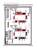
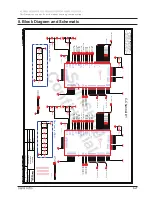
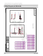
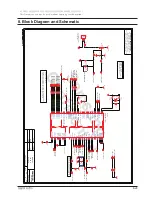
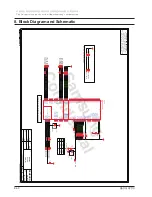
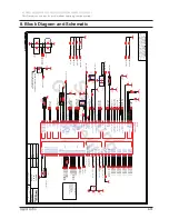
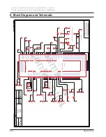
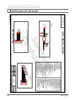
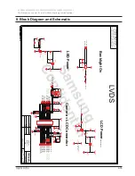
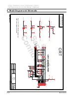
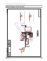
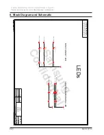
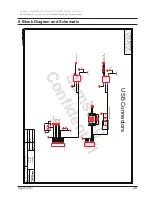
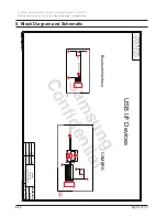
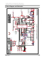
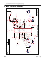
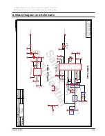
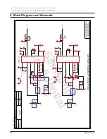
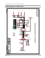
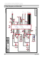
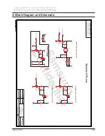
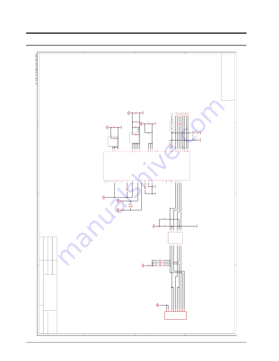
8. Block Diagram and Schematic
- 이 문서는 삼성전자의 기술 자산으로 승인자만이 사용할 수 있습니다 -
- This Document can not be used without Samsung's authorization -
Samsung
Confidential
Samsung
Confidential
Samsung
Confidential
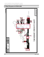
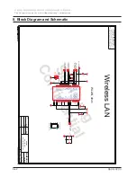
Place AC coupling capacitors
Place nearby PIN
1
Place crystal within 0.75inches from LAN Chip
DESIGN
Need at least 2.5mm or more Clearance
1
from conductive material
PAGE
D
PART NO
.
OF
B
A
LAST EDIT
A
SAMSUN
G
CHECK
TITLE
4
ELECTRONICS
2
4
C
RE
V
DAT
E
EXCEPT AS AUTHORIZED BY SAMSUNG
.
2
3
B
THIS DOCUMENT CONTAINS CONFIDENTIA
L
DEV. STEP
SAMSUNG PROPRIETAR
Y
DO NOT DISCLOSE TO OR DUPLICATE FOR OTHER
S
D
3
C
PROPRIETARY INFORMATION THAT IS
1
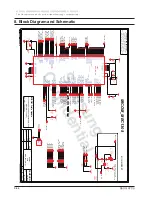
Place nearby PIN 29
Jun PARK
YM.AHN
HJ.KIM
9/23/2008
PV
1.0
October 27, 2009 14:27:43 PM
BA41-xxxxxA
40
59
Bremen-
L
LAN
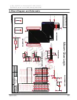
LAN_MARVELL_805
7
D:/users/mobile24/mentor/Bremen-L/PV/Bremen-L_MAI
N
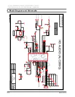
LAN Controller (88E8040)
Close to LAN Chip
SAMSUNG ELECTRONICS CO’S PROPERTY.
MODULE CODE
APPROVAL
0.01nF
C68
0.5pF
50
V
10
K
R5
3
P3.3V
C6
5
100nF
10V
nostuf
f
R36
1K
1%
3K
V
C5
9
9
MNT1
MNT2
10
3
RD
+
RD
-
6
1
TD
+
TD
-
2
TERM
1
4
5
TERM
2
7
TERM
3
TERM
4
8
P2.5V_LAN
1n
F
14
TD+
7
8
TD-
6
TDCT
TX+
10
9
TX-
11
TXCT
P2.5V_LA
N
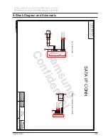
3722-00286
5
J512
JACK-LAN-8P
LFE8423 LT501
RD+
1
2
RD- RDCT
3
RX+
16
15
RX-
RXCT
1%
1K
R40
C
57
2
10
0n
F
10
V
P1.2V_LAN
C
57
9
10
V
10
0n
F
10V
100nF
C6
9
P3.3V_AUX
P3.3V
C74
100nF
10V
25MH
z
Y1
1
2
1%
R47
2K
C7
0
100nF
10V
10
V
C616
4700nF-X5R
4700nF-X5R
C6
4
10
V
100nF
C6
3
C7
3
100nF
10V
10V
R5
0
10
K
0
R5
2
P3.3V_AUX
1%
1%
4.7K
R5
6
nostuf
f
100nF
C618 C617
100nF
10V
30-B4
11-B1
10V
30-A4
44-C3
31-C4,42-C3
30-B4
13-B1,19-D
4
11-B1
11-B1
30-A4
VDD5
7
VDDO_TTL
1
30
VDDO_TTL
2
46
VDDO_TTL3
36
VMAIN_AVLBL
28
VPD_CLK
31
VPD_DATA
5
WAKE
#
11
XTAL
I
10
XTAL
O
42-C2,44-B3
30-C1,34-A4
13
RX
P
35
TESTMOD
E
49
THERMAL
17
TX
N
16
TX
P
9
VAUX_AVLBL
2
VDD
1
6
VDD
2
23
VDD3
VDD4
34
29
RESERVED10
19
RESERVED
2
RESERVED
3
20
21
RESERVED
4
RESERVED
5
22
24
RESERVED
6
RESERVED
7
25
RESERVED
8
26
RESERVED
9
27
12
RSET
14
RX
N
LOM_DISABLE#
40
PCIE_RX
N
41
PCIE_RX
P
38
PCIE_TX
N
37
PCIE_TX
P
3
PD_12_2
5
4
PERST
#
33
PU_VDDO_TTL
43
REFCLK
N
42
REFCLK
P
RESERVED
1
18
47
1205-003904
88E8040-A0-NNB2C000 U504
1
AVDD2.5_OUT
15
AVDD
L
39
AVDDL25
32
CLKREQ#
44
LED_ACT#
48
LE
D
_L
IN
K#
LED_SPEED
#
45
8
3.465V
R39
1K
1%
1%
1K
R38
P3.3V_AUX
PEX1_LAN_RXN
4
LAN3_CLKREQ#
LAN1_TXCT_M
N
LAN1_RXCT_MN
LAN1_CABLE_TERMINATION2_M
N
LAN1_CABLE_TERMINATION1_M
N
LAN3_DISABLE#_R_MN
50
V
0.5pF
C67
0.01n
F
LAN1_TXN_MN
LAN1_RXP_M
N
LAN1_TXP_MN
LAN1_RXN_MN
PEX1_LAN_TXN4 PEX1_LAN_TXP4
PEX1_LAN_RXN4_C_M
N
PEX1_LAN_RXP4_C_M
N
PLT3_RST
#
LAN3_PU_VDDO_R_MN
CLK1_PCIELOM
#
CLK1_PCIELOM
LAN3_RSET_M
N
PEX3_WAKE#
LAN3_XTALI_M
N
LAN3_XTALO_MN
PEX1_LAN_RXP4
Summary of Contents for R530
Page 5: ...iii Contents This Document can not be used without Samsung s authorization R530 R730...
Page 64: ...6 40 6 Material List This Document can not be used without Samsung s authorization R530 R730...
Page 240: ...4 23 4 Troubleshooting This Document can not be used without Samsung s authorization R530 R730...
Page 241: ...4 24 4 Troubleshooting This Document can not be used without Samsung s authorization R530 R730...
Page 249: ...4 32 4 Troubleshooting This Document can not be used without Samsung s authorization R530 R730...


