UPI-41A/41AH/42/42AH USER’S MANUAL
231318 – 39
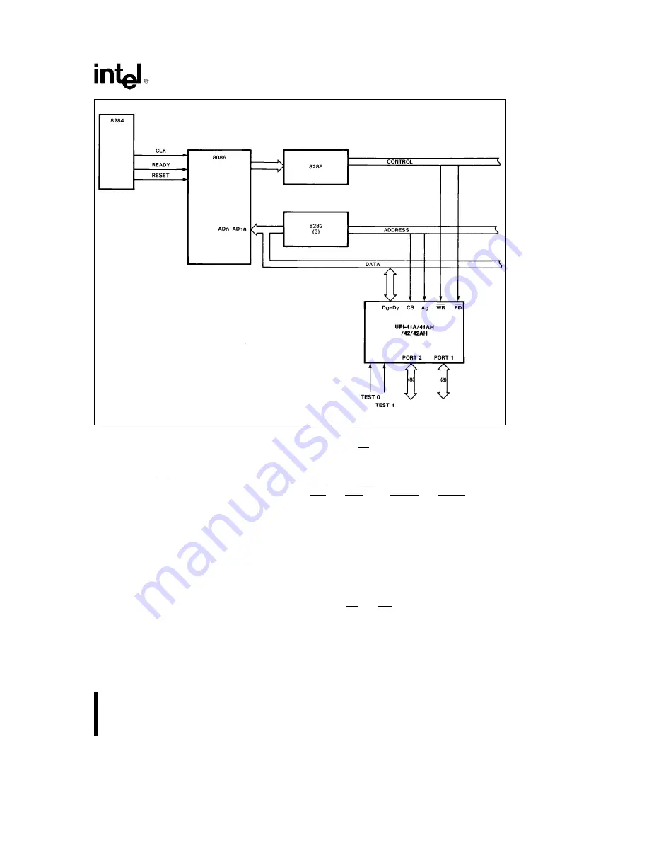
Figure 5-8. 8086-UPI Maximum Mode Systems
8282 latches providing separate address and data buses.
The address bus is 20-lines wide and the data bus is 16-
lines wide. Multiplexed control lines are decoded by the
8288. The UPI’s CS input is provided by linear selec-
tion. Note that the UPI is both I/O mapped and memo-
ry mapped as a result of the linear addressing tech-
nique. An address decoder may be used to limit the
UPI-41A/41AH/42/42AH to a specific I/O mapped
address. Address line A
1
is connected to the UPI’s A
0
input. This insures that the registers of the UPI will
have even I/O addresses. Data will be transferred on
D
0
– D
7
lines only. This allows the I/O registers to be
accessed using byte manipulation instructions.
8080 Interface
Figure 5-9 illustrates the interface to an 8080A system.
In this example, a crystal and capacitor are used for
UPI-41A/41AH/42/42AH timing reference and pow-
er-on RESET. If the 2-MHz 8080A 2-phase clock were
used instead of the crystal, the UPI-41A/41AH/42/
42AH would run at only 16% full speed.
The A
0
and CS inputs are direct connections to the
8080 address bus. In larger systems, however, either of
these inputs may be decoded from the 16 address lines.
The RD and WR inputs to the UPI can be either the
IOR and IOW or the MEMR and MEMR signals de-
pending on the I/O mapping technique to be used.
The UPI can be addressed as an I/O device using IN-
put and OUTput instructions in 8080 software.
8048 Interface
Figure 5-10 shows the UPI interface to an 8048 master
processor.
The 8048 RD and WR outputs are directly compatible
with the UPI. Figure 5-11 shows a distributed process-
ing system with up to seven UPI’s connected to a single
8048 master processor.
In this configuration the 8048 uses PORT 0 as a data
bus. I/O PORT 2 is used to select one of the seven
59


