Rev. 1.10
88
November 04, 2019
Rev. 1.10
89
November 04, 2019
HT45F5Q-3
Battery Charger Flash MCU
HT45F5Q-3
Battery Charger Flash MCU
Analog to Digital Converter
The need to interface to real world analog signals is a common requirement for many electronic
systems. However, to properly process these signals by a microcontroller, they must first be
converted into digital signals by A/D converters. By integrating the A/D conversion electronic
circuitry into the microcontroller, the need for external components is reduced significantly with the
corresponding follow-on benefits of lower costs and reduced component space requirements.
A/D Converter Overview
This device contains a multi-channel analog to digital converter which can directly interface to
external analog signals, such as that from sensors or other control signals, or internal analog signals,
such as the OPA2 output voltage, 20×A2P, and convert these signals directly into a 12-bit digital
value. The external or internal analog signal to be converted is determined by the SAINS2~SAINS0
bits together with the SACS3~SACS0 bits. More detailed information about the A/D input signal
is described in the “A/D Converter Control Registers” and “A/D Converter Input Signals” sections
respectively.
External Input Channels
Internal Input Signals
A/D Input Select Bits
AN0~AN9
20×A2P
SAINS2~SAINS0,
SACS3~SACS0
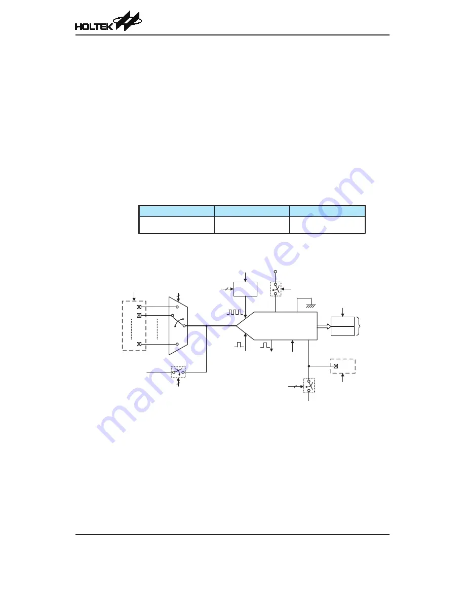
The accompanying block diagram shows the overall internal structure of the A/D converter, together
with its associated registers.
A/D Converter
START
ADBZ ADCEN
V
SS
A/D Clock
÷2
N
(N=0~7)
f
SYS
V
DD
ADCEN
SADOL
SADOH
AN9
A/D Converter
Reference Voltage
A/D Data
Registers
ADRFS
SACS3~
SACS0
SACKS2~
SACKS0
Pin-shared
Selection
Pin-shared
Selection
V
DD
SAVRS1~
SAVRS0
VREF
AN0
AN1
SAINS2~SAINS0
20×A2P
A/D Converter Structure
Note: 20×A2P is 20 times OPA2 positive input voltage signal. More details can be obtained in the
Battery Charge Module section.


