Epson Research and Development
Page 85
Vancouver Design Center
Hardware Functional Specification
S1D13704
Issue Date: 01/02/08
X26A-A-001-04
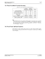
13.3 Power Save Mode Function Summary
Note
When FPDAT[11:8] are designated as GPIO outputs, the output state prior to enabling
the Power Save Mode is maintained. When FPDAT[11:8] are designated as GPIO in-
puts, unused inputs must be tied to either IO V
DD
or GND - see Table 5-3: “LCD Inter-
face Pin Mapping,” on page 23.
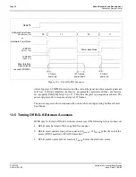
13.4 Panel Power Up/Down Sequence
After chip reset or when entering/exiting a power save mode, the Panel Interface signals
follow a power on/off sequence shown below. This sequence is essential to prevent damage
to the LCD panel.
Table 13-4: Power Save Mode Function Summary
Hardware
Power Save
Software
Power Save
Normal
IO Access Possible?
No
Yes
Yes
Memory Access Possible?
No
Yes
Yes
Sequence Controller Running?
No
No
Yes
Display Active?
No
No
Yes
LCDPWR
Inactive
Inactive
Active
FPDAT[11:0], FPSHIFT (see note)
Forced Low
Forced Low
Active
FPLINE, FPFRAME, DRDY
Forced Low
Forced Low
Active
*

