Epson Research and Development
Page 13
Vancouver Design Center
Interfacing to the Motorola MC68328 ‘Dragonball’ Microprocessor
S1D13704
Issue Date: 01/02/12
X26A-G-007-03
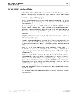
4.1.2 Using The Generic #1 Host Bus Interface
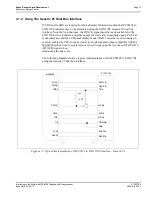
If UDS and/or LDS are required for their alternate IO functions, then the MC68328 to
S1D13704 interface may be implemented using the S1D13704 Generic #1 host bus
interface. Note that in either case, the DTACK signal must be made available for the
S1D13704, since it inserts a variable number of wait states depending upon CPU/LCD
synchronization and the LCD panel display mode. WAIT# must be inverted (using an
inverter enabled by CS#) to make it an active high signal and thus compatible with the
MC68328 architecture. A single resistor is used to speed up the rise time of the WAIT#
(DTACK) signal when
terminating the bus cycle.
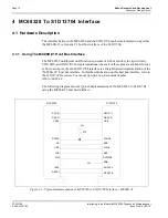
The following diagram shows a typical implementation of the MC68328 to S1D13704
using the Generic #1 host bus interface.
Figure 4-2: Typical Implementation of MC68328 to S1D13704 Interface - Generic #1
MC68328
S1D13704
A[15:0]
D[15:0]
DTACK
UWE
LWE
OE
CLK0
RESET
AB[15:0]
DB[15:0]
CS#
WAIT#
WE1#
WE0#
RD/WR#
RD#
BUSCLK
RESET#
Vcc
470
CSB3
*


