Page 36
Epson Research and Development
Vancouver Design Center
S1D13704
Hardware Functional Specification
X26A-A-001-04
Issue Date: 01/02/08
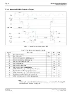
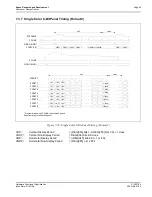
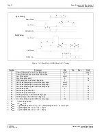
7.3.2 Power Down/Up Timing
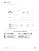
Figure 7-9: Power Down/Up Timing
Table 7-8: Power Down/Up Timing
Symbol
Parameter
Min
Typ
Max
Units
t1
HW Power Save active to FPLINE, FPFRAME, FPSHIFT, FPDAT, DRDY
inactive - LCDPWR Override = 1
1
Frame
t2
HW Power Save inactive to FPLINE, FPFRAME, FPSHIFT, FPDAT, DRDY
active - LCDPWR Override = 1
1
Frame
t3
HW Power Save active to FPLINE, FPFRAME, FPSHIFT, FPDAT, DRDY
inactive - LCDPWR Override = 0
1
Frame
t4
LCDPWR low to FPLINE, FPFRAME, FPSHIFT, FPDAT, DRDY inactive
- LCDPWR Override = 0
127
Frame
t5
HW Power Save inactive to FPLINE, FPFRAME, FPSHIFT, FPDAT, DRDY,
LCDPWR active - LCDPWR Override = 0
0
Frame
t6
LCDPWR Override active (1) to LCDPWR inactive
1
Frame
t7
LCDPWR Override inactive (1) to LCDPWR active
1
Frame
t4
t3
t1
Active
Inactive
Active
Inactive
Active
LCDPWR Override
(REG[03h] bit 3)
HW Power Save
FP Signals
LCDPWR
t2
Software Power Save
11
00
11
00
11
t5
t6
t7
(polarity set by CNF4)
REG[03h] bits [1:0]
or
Active
Active
Active
Inactive
Inactive
*

