EPSON Research and Development
Page 11
Vancouver Design Center
Interfacing to the Toshiba MIPS TX3912 Processor
S1D13704
Issue Date: 01/02/12
X26A-G-004-02
The “Generic #1” host interface control signals of the S1D13704 are asynchronous with respect to
the S1D13704 bus clock. This gives the system designer full flexibility to choose the appropriate
source (or sources) for CLKI and BCLK. The choice of whether both clocks should be the same, and
whether to use DCLKOUT (divided) as clock source, should be based on pixel and frame rates,
power budget, part count and maximum S1D13704 respective clock frequencies. Also, internal
S1D13704 clock dividers provide additional flexibility.
3.2 IT8368E Configuration
The IT8368E provides eleven multi-function IO pins (MFIO). The IT8368E must have both “Fix
Attribute/IO” and “VGA” modes on. When both these modes are enabled, the MFIO pins provide
control signals needed by the S1D13704 host bus interface, and a 16M byte portion of the system
PC Card attribute and IO space is allocated to address the S1D13704. When accessing the S1D13704
the associated card-side signals are disabled in order to avoid any conflicts.
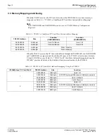
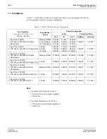
For mapping details, refer to section 3.3: “Memory Mapping and Aliasing.” For connection details
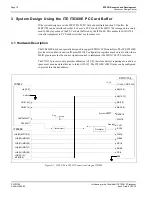
see Figure 3-1: “S1D13704 to TX3912 Connection Using an IT8368E,” on page 10. For further
information on the IT8368E, refer to the IT8368E PC Card/GPIO Buffer Chip Specification.
Note
When a second IT8368E is used, that circuit should not be set in VGA mode.
*

