7 OSCILLATOR CIRCUIT (OSC)
68
EPSON
S1C17001 TECHNICAL MANUAL
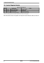
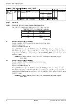
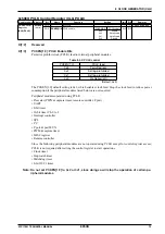
0x5064: FOUT Control Register (OSC_FOUT)
Register name Address
Bit
Name
Function
Setting
Init. R/W
Remarks
FOUT Control
Register
(OSC_FOUT)
0x5064
(8 bits)
D7–4
–
reserved
–
–
–
0 when being read.
D3–2
FOUT3D[1:0]
FOUT3 clock division ratio select
FOUT3D[1:0]
Division ratio
0x0
R/W
0x3
0x2
0x1
0x0
reserved
OSC3-1/4
OSC3-1/2
OSC3-1/1
D1
FOUT3E
FOUT3 output enable
1 Enable
0 Disable
0
R/W
D0
FOUT1E
FOUT1 output enable
1 Enable
0 Disable
0
R/W
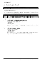
D[7:4] Reserved
D[3:2]
FOUT3D[1:0]: FOUT3 Clock Division Ratio Select Bits
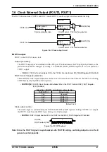
Select the OSC3 clock division ratio to set the FOUT3 clock frequency.
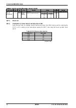
Table 7.8.3: FOUT3 clock division ratio selection
FOUT3D[1:0]
Division ratio
0x3
Reserved
0x2
OSC3-1/4
0x1
OSC3-1/2
0x0
OSC3-1/1
(Default: 0x0)
D1
FOUT3E: FOUT3 Output Enable Bit
Permits or prohibits FOUT3 clock (OSC3 division clock) external output.
1 (R/W): Permitted (on)
0 (R/W): Prohibited (off) (default)
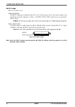
Setting FOUT3E to 1 outputs the FOUT3 clock from the FOUT3 pin. Setting it to 0 stops the output.
The FOUT3 output pin is combined with the P30 port. This functions as the P30 port pin by default, so
the pin function should be changed by writing 1 to P30MUX (D0/P3_PMUX register) if use is required
for FOUT3 output.
∗
P30MUX
: P30 Port Function Select Bit in the P3 Port Function Select (P3_PMUX) Register
(D0/0x52a3)
D0
FOUT1E: FOUT1 Output Enable Bit
Permits or prohibits FOUT1 clock (OSC1 clock) external output.
1 (R/W): Permitted (on)
0 (R/W): Prohibited (off) (default)
Setting FOUT1E to 1 outputs the FOUT1 clock from the FOUT1 pin. Setting it to 0 stops the output.
The FOUT1 output pin is combined with the P13 port. This functions as the P13 port pin by default, so
the pin function should be changed by writing 1 to P13MUX (D3/P1_PMUX register) if use is required
for FOUT1 output.
∗
P13MUX
: P13 Port Function Select Bit in the P1 Port Function Select (P1_PMUX) Register
(D3/0x52a1)
Summary of Contents for S1C17001
Page 1: ...Technical Manual S1C17001 CMOS 16 BIT SINGLE CHIP MICROCONTROLLER ...
Page 33: ...4 POWER SUPPLY VOLTAGE 24 EPSON S1C17001 TECHNICAL MANUAL This page intentionally left blank ...
Page 63: ...6 INITERRUPT CONTROLLER 54 EPSON S1C17001 TECHNICAL MANUAL This page intentionally left blank ...
Page 87: ...8 CLOCK GENERATOR CLG 78 EPSON S1C17001 TECHNICAL MANUAL This page intentionally left blank ...
Page 91: ...9 PRESCALER PSC 82 EPSON S1C17001 TECHNICAL MANUAL This page intentionally left blank ...
Page 133: ...11 16 BIT TIMER T16 124 EPSON S1C17001 TECHNICAL MANUAL This page intentionally left blank ...
Page 211: ...16 STOPWATCH TIMER SWT 202 EPSON S1C17001 TECHNICAL MANUAL This page intentionally left blank ...
Page 219: ...17 WATCHDOG TIMER WDT 210 EPSON S1C17001 TECHNICAL MANUAL This page intentionally left blank ...
Page 241: ...18 UART 232 EPSON S1C17001 TECHNICAL MANUAL This page intentionally left blank ...
Page 277: ...20 I2 C 268 EPSON S1C17001 TECHNICAL MANUAL This page intentionally left blank ...
Page 313: ...25 PACKAGE 304 EPSON S1C17001 TECHNICAL MANUAL This page intentionally left blank ...


