Epson DFX-9000
Revision B
Operating Principles
Circuit operation
89
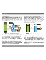
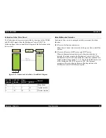
The offset time is the sum of the following four offset values.
Offset time = Speed FR constant flight time
offset
Speed offset
Offset value to correct for CR speed differences.
Front/Rear (FR) offset
Offset value to correct for the flight time difference between the
front head and rear head.
Constant offset
Offset value to correct for the difference between the pin pitch and
print density.
Flight time offset
Offset value to correct for the individual flight time for each pin.
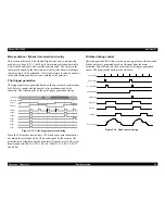
In addition, a parallel timer is used to reduce the conducting time to even
out the impact of one pin when that pin is used repeatedly in a job. If an
operation of the pin is detected in the previous print cycle, the “parallel
enable” and the mask signal are activated to reduce the main excitation
time. The Mechanism Control ASIC then outputs a main excitation
control signal (MAINF_xx) and flyback signal (FLYBK_xx) to activate
the transistor to control the printhead.
Head abnormal current detection circuit
When an abnormal current exceeding the prescribed level is detected,
the status is sent to the Mechanism Control ASIC. If the Mechanism
Control ASIC internal circuit detects that the status has continued for a
certain period of time, the 42 V/37 V line for the ROM board is cut off
by turning the X42VPST signal off (low). The firmware recognizes this
state when it performs a Read operation on the Mechanism Control
ASIC internal register.
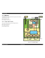
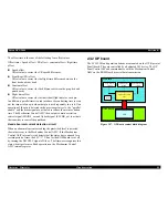
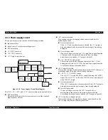
2.3.2 OP board
The LCD, LED and operation buttons are mounted on the OP (Operator
Panel) board. They are controlled by a dedicated LSI device. The OP
Panel Control LSI and communicates with the Mechanism Control
ASIC on the ROM Board by serial data transmission.
Figure 2-37. OP Board control block diagram
LED display
section
LCD display
section
Switch operation
section
OP Panel Control
LSI
OP Board
ROM Board
ASIC
Buzzer
Summary of Contents for DFX-9000
Page 1: ...EPSONDFX 9000 Serial Impact Dot Matrix Printer SEDM04003 SERVICE MANUAL ...
Page 8: ...C H A P T E R 1 PRODUCT DESCRIPTION ...
Page 61: ...Epson DFX 9000 Revision B Product Description Dimensions and weight 54 ...
Page 62: ...C H A P T E R 2 OPERATING PRINCIPLES ...
Page 99: ...Epson DFX 9000 Revision B Operating Principles Circuit operation 92 ...
Page 100: ...C H A P T E R 3 TROUBLESHOOTING ...
Page 104: ...Epson DFX 9000 Revision B Troubleshooting Overview 97 Mechanism initialization e e e e e ...
Page 107: ...Epson DFX 9000 Revision B Troubleshooting Overview 100 PAPER FEEDING FF APG APPROACH ...
Page 130: ...C H A P T E R 4 DISASSEMBLY AND ASSEMBLY ...
Page 218: ...C H A P T E R 5 ADJUSTMENT ...
Page 263: ...Epson DFX 9000 Revision B Adjustment Additional functions 256 ...
Page 264: ...C H A P T E R 6 MAINTENANCE ...
Page 286: ...C H A P T E R 7 APPENDIX ...
Page 297: ......
Page 298: ......
Page 299: ......
Page 300: ......
Page 301: ......
Page 302: ......
Page 303: ......
Page 304: ......
Page 305: ......
Page 306: ......
Page 307: ......
Page 308: ......
Page 309: ......
Page 310: ......
Page 311: ......
Page 312: ......
Page 313: ......
Page 314: ......
Page 315: ......
Page 316: ......
Page 317: ......
Page 318: ......
Page 319: ......
Page 320: ......
Page 321: ......
Page 322: ......
Page 323: ......
Page 324: ...EPSON DFX 9000 Revision B Appendix Component Layout 317 7 4 Component Layout ...
Page 333: ...EPSON DFX 9000 Revision B Appendix Parts list 326 ...

