


Appendix
Appendix 2 Time Domain Measurement
347
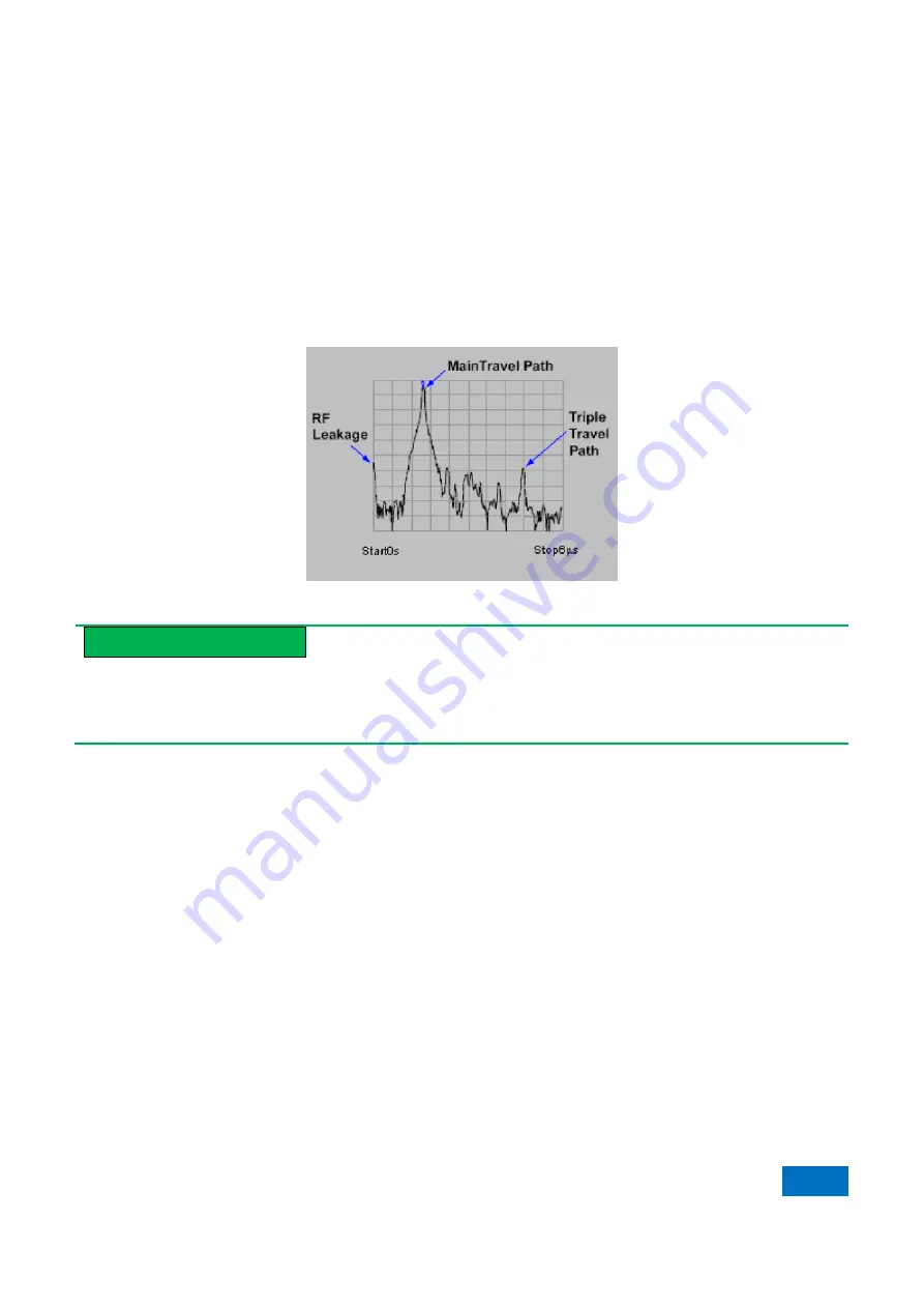
1) Refer to the transmission loss or gain in the LOGMAG mode.
2) Refer to the transmission coefficient in the LINMAG mode.
Fig. 2.17 shows an example of transmission measurement in the band-pass mode.
3) This example shows the information of multiple paths transmitted in the SAW (surface acoustic wave) filter in
the selected mode.
4) The pulse which is the closest to the time point 0 refers to the transmission time of on the shortest path from the
output to input of the network analyzer. It may be or not be the largest pulse or best transmission path.
5) Each concurrent pulse may be transmitted in other paths from the input to output. However, such paths are all
longer than the shortest path.
Fig. 2.17 Transmission Measurement in Band-pass Mode
Prompt
Observation of the main path of SAW filter response:
In order to see the main channel of SAW filter response, you can set the gate to block all pulses except main pulses.
Only the frequency response of the main path can be displayed in the frequency domain.
2.5.4 Error Positioning of Low-Pass Mode
The response of the time domain reflectometer (TDR) can be simulated in the low-pass test mode. It includes all
useful and decisive information of the breaking point. The following figure shows the low-pass response of the
known breaking point. The waveform of each circuit element is simulated corresponding to the S
11
response of the
low-pass time domain mode. You are allowed to observe the step response or pulse stimulus pulse in the low-pass
mode.
Summary of Contents for AV3672 Series
Page 3: ......
Page 4: ...AV3672 Series Vector Network Analyzer Contents...
Page 5: ......
Page 124: ...5 Menu 5 1 Menu structure 120 5 1 2 Track Fig 5 2 Track Menu...
Page 125: ...5 Menu 5 1 Menu structure 121 5 1 3 Channel Fig 5 3 Channel Menu...
Page 126: ...5 Menu 5 1 Menu structure 122 5 1 4 Excitation Fig 5 4 Excitation Menu I...
Page 127: ...5 Menu 5 1 Menu structure 123 Fig 5 5 Excitation Menu II...
Page 128: ...5 Menu 5 1 Menu structure 124 Fig 5 6 Excitation Menu III...
Page 129: ...5 Menu 5 1 Menu structure 125 5 1 5 Response Fig 5 7 Response Menu I...
Page 130: ...5 Menu 5 1 Menu structure 126 Fig 5 8 Repsonse Menu II...
Page 131: ...5 Menu 5 1 Menu structure 127 Fig 5 9 Response Menu III...
Page 132: ...5 Menu 5 1 Menu structure 128 Fig 5 10 Response Menu V Fig 5 11 Response IV...
Page 133: ...5 Menu 5 1 Menu structure 129 5 1 6 Calibration Fig 5 12 Calibration Menu...
Page 134: ...5 Menu 5 1 Menu structure 130 5 1 7 Marker Fig 5 13 Cursor Menu I...
Page 135: ...5 Menu 5 1 Menu structure 131 Fig 5 13 Cursor Menu II...
Page 136: ...5 Menu 5 1 Menu structure 132 Fig 5 15Marker Menu III...
Page 137: ...5 Menu 5 1 Menu structure 133 5 1 8 Analysis Fig 5 16 Analysis Menu I...
Page 138: ...5 Menu 5 1 Menu structure 134 Fig 5 17 Analysis Menu II...
Page 139: ...5 Menu 5 1 Menu structure 135 Fig 5 18 Analysis Menu III...
Page 140: ...5 Menu 5 1 Menu structure 136 5 1 9 System Fig 5 19 System Menu I...
Page 141: ...5 Menu 5 1 Menu structure 137 Fig 5 20 System Menu I...
Page 254: ...8 Basis of Network Measurement 8 3 Amplifier Parameter Specifications 250...
Page 257: ...8 Basis of Network Measurement 8 4 Complex Impedance 253...
Page 373: ...Appendix Appendix 4 Pulse Measurement 369 Fig 4 9 Receiver gain configuration Dialog Box...


