VIII-84
I-24
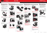
Uneven Density (Right & Left)
Phenomenon
The optical density is different between the right and left side of the printed image.
Main Causes
1) The amount of toner in the toner cartridge PU is short.
2) The retract operation of the toner cartridge PU is not properly done.
3) The belt of the toner cartridge PU is deformed.
4) The belt of the transfer unit is deformed.
5) The transfer roller ASSY PU is not properly installed.
6) The rear cover ASSY PU is deformed.
7) The rear cover ASSY PU is not locked sufficiently
8) The dustproof glass of laser ASSY PU is stained.
Belt Cartridge PU
Rear Cover Assy PU
Transfer Belt
Toner Cartridge PU
Transfer Unit PU
Laser Unit Assy PU
Countermeasures
1) Replace the toner cartridge PU.
2) Check the toner retract clutch PU.
3) Replace the belt cartridge PU.
4) Confirm the proper installation of the transfer roller ASSY PU.
5) Replace the transfer roller ASSY PU.
6) Ensure to lock the rear cover ASSY PU.
7) Replace the rear cover ASSY PU.
8) Clean the laser ASSY PU.
9) Replace the laser ASSY PU.
Summary of Contents for HL-2700CN Series
Page 16: ...viii 3 Rating Label 6 0A 11 0A For Europe For US ...
Page 18: ...CHAPTER I PRODUCT OUTLINE ...
Page 27: ...CHAPTER II SPECIFICATIONS ...
Page 39: ...III 1 CHAPTER III INSTALLATION ...
Page 53: ...CHAPTER IV STRUCTURE OF SYSTEM COMPONENTS ...
Page 84: ...IV 31 Layout of Clutches and Solenoids 1 2 3 4 5 6 7 8 9 10 Fig 4 30 ...
Page 90: ...IV 37 ...
Page 93: ...IV 40 c Interface Circuit Printer side Table 4 1 Interface Circuit ...
Page 102: ...IV 49 Main PCB circuit Diagram 1 7 IV 49 CODE B512168CIR 1 7 LJ9515001 NAME ...
Page 103: ...IV 50 Main PCB circuit Diagram 2 7 IV 50 CODE B512168CIR 2 7 LJ9515001 NAME ...
Page 104: ...IV 51 Main PCB circuit Diagram 3 7 IV 51 CODE B512168CIR 3 7 LJ9515001 NAME ...
Page 105: ...IV 52 Main PCB circuit Diagram 4 7 IV 52 CODE B512168CIR 4 7 LJ9515001 NAME ...
Page 106: ...IV 53 Main PCB circuit Diagram 5 7 IV 53 CODE B512168CIR 5 7 LJ9515001 NAME ...
Page 107: ...IV 54 Main PCB circuit Diagram 6 7 IV 54 CODE B512168CIR 6 7 LJ9515001 NAME ...
Page 108: ...IV 55 Main PCB circuit Diagram 7 7 IV 55 CODE B512168CIR 7 7 LJ9515001 NAME ...
Page 110: ...IV 57 Layout of Connector Pin Assignment Power Supply Unit Fig 4 40 ...
Page 118: ...IV 65 1 MCTL P W B I1CN IOD P W B DCN1 2 MCTL P W B I2CN IOD P W B DCN3 ...
Page 124: ...IV 71 30 Duplex Connector 31 Lower Feeder Connector 32 DCN2 IOD 33 DCN8 IOD LaserFan ...
Page 125: ...CHAPTER V CONTROL PANEL OPERATION ...
Page 171: ...CHAPTER VI PERIODIC MAINTENANCE ...
Page 197: ...CHAPTER VII DISASSEMBLY ...
Page 200: ...VII 3 Table 7 1 Table of Applicable Screws ...
Page 257: ...CHAPTER VIII TROUBLESHOOTING ...
Page 316: ...VIII 59 5 IMAGE FAILURE 1 2 3 4 5 6 7 8 9 10 11 12 13 14 ...
Page 317: ...VIII 60 15 a 15 b 16 17 18 19 20 21 22 23 24 25 Fig 8 2 ...
Page 346: ...A 4 6 Transfer Unit X X X X X X 7 1 2 3 Location DATE MONTH SERIAL NO YEAR ...


