V-39
48
EACH IMAGE SET
This mode can reset the number of total pages of each color on NVRAM whenever
executing NVRAM INITIAL or replacing the MCTL PWB.
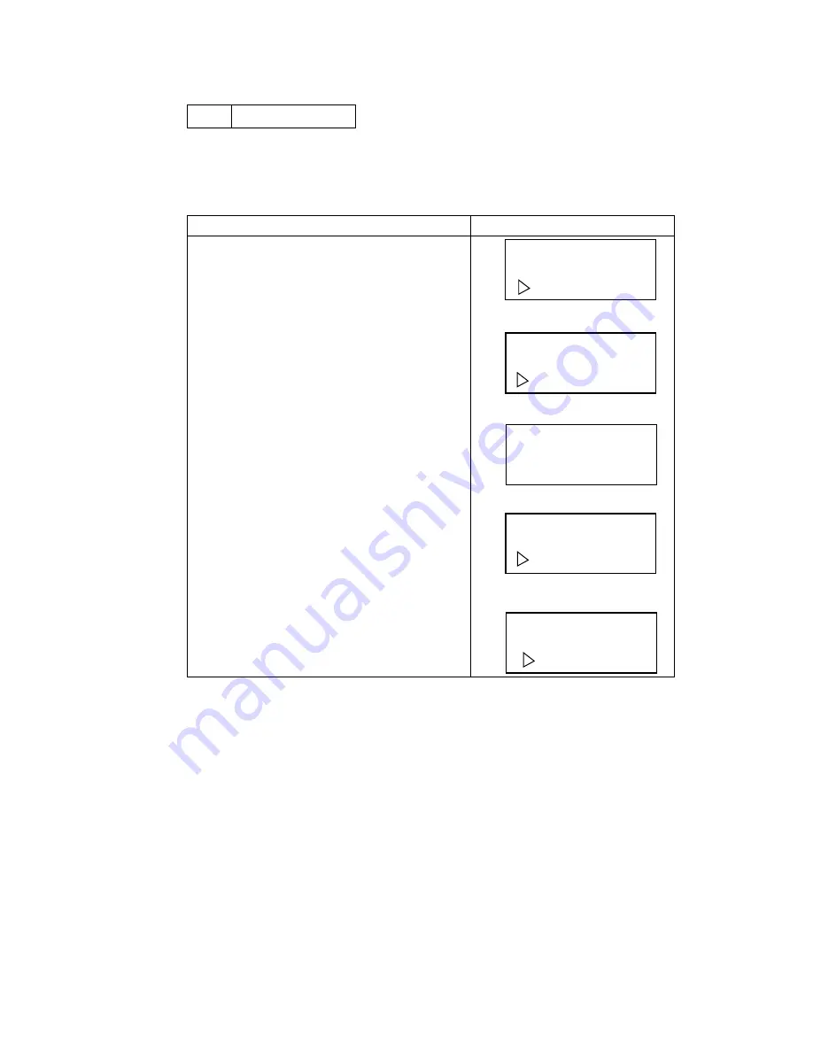
Description of Procedures
LCD Message
1) Press Set key after selecting EACH IMAGE
SET. (a)
→
(b)
2) Select the desired color subject to EACH
IMAGE SET. (b)
→
(c)
3) Use Back and + keys to designate or change
the desired digit.
Use Set key to input values to the blinking
digit.
Upon completing the input of values to be
set, use the Back and + keys to move the
cursor to SET displayed in the LCD, and
then, press the Set key to register the set
value. (c)
→
(d)
4) Press the - key to wrap up the EACH IMAGE
SET mode. (d)
→
(e)
39 FACTORY MODE
EACH IMAGE SET
48 IMAGE OF
Y / M / C / K
(a)
(b)
(c)
48 IMAGE OF C
0 0 5 4 3 2 P SET
39 FACTORY MODE
MARGIN ADJUST
(e)
48 IMAGE OF
Y / M / C / K
(d)
Summary of Contents for HL-2700CN Series
Page 16: ...viii 3 Rating Label 6 0A 11 0A For Europe For US ...
Page 18: ...CHAPTER I PRODUCT OUTLINE ...
Page 27: ...CHAPTER II SPECIFICATIONS ...
Page 39: ...III 1 CHAPTER III INSTALLATION ...
Page 53: ...CHAPTER IV STRUCTURE OF SYSTEM COMPONENTS ...
Page 84: ...IV 31 Layout of Clutches and Solenoids 1 2 3 4 5 6 7 8 9 10 Fig 4 30 ...
Page 90: ...IV 37 ...
Page 93: ...IV 40 c Interface Circuit Printer side Table 4 1 Interface Circuit ...
Page 102: ...IV 49 Main PCB circuit Diagram 1 7 IV 49 CODE B512168CIR 1 7 LJ9515001 NAME ...
Page 103: ...IV 50 Main PCB circuit Diagram 2 7 IV 50 CODE B512168CIR 2 7 LJ9515001 NAME ...
Page 104: ...IV 51 Main PCB circuit Diagram 3 7 IV 51 CODE B512168CIR 3 7 LJ9515001 NAME ...
Page 105: ...IV 52 Main PCB circuit Diagram 4 7 IV 52 CODE B512168CIR 4 7 LJ9515001 NAME ...
Page 106: ...IV 53 Main PCB circuit Diagram 5 7 IV 53 CODE B512168CIR 5 7 LJ9515001 NAME ...
Page 107: ...IV 54 Main PCB circuit Diagram 6 7 IV 54 CODE B512168CIR 6 7 LJ9515001 NAME ...
Page 108: ...IV 55 Main PCB circuit Diagram 7 7 IV 55 CODE B512168CIR 7 7 LJ9515001 NAME ...
Page 110: ...IV 57 Layout of Connector Pin Assignment Power Supply Unit Fig 4 40 ...
Page 118: ...IV 65 1 MCTL P W B I1CN IOD P W B DCN1 2 MCTL P W B I2CN IOD P W B DCN3 ...
Page 124: ...IV 71 30 Duplex Connector 31 Lower Feeder Connector 32 DCN2 IOD 33 DCN8 IOD LaserFan ...
Page 125: ...CHAPTER V CONTROL PANEL OPERATION ...
Page 171: ...CHAPTER VI PERIODIC MAINTENANCE ...
Page 197: ...CHAPTER VII DISASSEMBLY ...
Page 200: ...VII 3 Table 7 1 Table of Applicable Screws ...
Page 257: ...CHAPTER VIII TROUBLESHOOTING ...
Page 316: ...VIII 59 5 IMAGE FAILURE 1 2 3 4 5 6 7 8 9 10 11 12 13 14 ...
Page 317: ...VIII 60 15 a 15 b 16 17 18 19 20 21 22 23 24 25 Fig 8 2 ...
Page 346: ...A 4 6 Transfer Unit X X X X X X 7 1 2 3 Location DATE MONTH SERIAL NO YEAR ...


