


AD9361 Reference Manual
UG-570
| Page 85 of 128
GENERAL PURPOSE OUTPUT CONTROL
The
AD9361
has four GPO pins that can be setup using the
ad9361_gpo_setup function. The GPOs commonly control
antenna switches or LNA enable. There are two options for
controlling the GPOs. The manual method uses SPI writes
from the BBP. The automatic method slaves the GPOs to the
enable state machine (ENSM). When using external LNAs, the
AD9361
can optionally slave GPO_0 and GPO_1 off the receive
gain tables to control LNA gain on each of the two receivers.
The supply voltage to the GPOs comes from a pin VDD_GPO
(B8) on the
AD9361
with a nominal supply voltage range of
1.3 V to 3.3 V. Setting Bit D4 of Register 0x026 puts the GPOs
in manual control mode. Use the upper nibble (four bits) of
Register 0x027 as the GPO logic level controls. GPO_3 uses D7;
GPO_2 uses D6, GPO_1 uses D5, GPO_0 uses D4. In this
mode, the lower nibble of Register 0x26 is ignored.
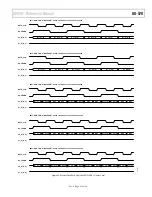
GPO Auto Toggle
When initializing the GPOs for ENSM Control the initial states
of the GPOs should be set in the lower nibble of Register 0x27
with GPO_0 corresponding to Bit D0, GPO_1 corresponding to
Bit D1, GPO_2 corresponding to Bit D2 and GPO_3
corresponding to Bit D3. Register 0x20 contains the bits that
determine how the GPOs respond to state changes from Alert.
The upper nibble controls, which GPO pins, will change states
when moving to Rx mode and the lower nibble controls, which
GPO pins, will change states in Tx. For example let Register
0x26 be 0x00 (ENSM control enabled), Register 0x27 be 0xFF
(initialize all GPO pins to 1), and Register 0x20 = 0x24(toggle
the GPO_1 pin in Rx and GPO_2 in Tx). When the part enters
alert state, all GPO pins will become high. When the part enters
Tx, only Pin GPO_2 pin will toggle low. When the part enters
Rx, GPO_1 pin will toggle low. This is a typical scenario for a
T/R switch with differential control.
Some applications have a need to insert a delay between the
DUT state transitions and GPO pin toggles. To accommodate
these needs, there are GPO registers that can be programmed to
the required delay. Register 0x28 through Register 0x2B set the
delay from an ENSM state change of alert to receive while
Register 0x02C through Register 0x02F set the delay from an
ENSM state change from Alert to Transmit. Each LSB is 1 µs.
The delay settings will only work when the TXNRX and
ENABLE pins are used to control the state machine. The delay
settings will not work when SPI is used to control the state
machine. Depending on the reference clock, program Register
0x3A for a resolution of 1 µs/LSB. Set Bits[D6:D0] to the
number of reference clock cycles per µs minus one. In FDD
mode, the Tx enable and Tx delays are applied while the Rx
enable and Rx delays are ignored.
Rev. A


