


AD9361 Reference Manual
UG-570
| Page 107 of 128
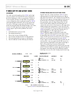
LVDS MODE DATA PATH SIGNALS
The data path interface consists of the following signals.
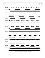
DATA_CLK
DATA_CLK is a differential LVDS signal generated in the
AD9361
and provided to the BBP as a master clock for the
Rx data path. The BBP uses this master clock as the timing
reference for the interface data transfers and for the baseband
processing of the data samples. DATA_CLK provides source-
synchronous timing with DDR operation for the Rx_D[5:0]
signals during receive operation. SDR is not available in LVDS
mode.
The frequency of DATA_CLK depends on the system
architecture (number of RF channels, degree of oversampling
and BW mode). This frequency is set via SPI writes to the
AD9361
.
DATA_CLK can be stopped by the
AD9361
(in response to a
SPI transaction from the BBP) during interface idle periods to
reduce power consumption. If DATA_CLK is disabled, the
transition to and from the nontoggling state must obey the
electrical layer requirements for clean signal transitions, and a
valid level must be driven by the
AD9361
at all times.
FB_CLK
FB_CLK is a differential LVDS signal driven from the BBP
and is a feedback (loop back) version of DATA_CLK. FB_CLK
provides source-synchronous timing with dual edge capture for
Tx_D[5:0] signals during Tx bursts.
FB_CLK can be stopped by the BBP during interface idle
periods to reduce power consumption. If so, the transitions to
and from the nontoggling state must obey the electrical layer
requirements for clean signal transitions, and a valid level must
be driven by the BBP at all times.
Rx_FRAME
Rx_FRAME is a differential LVDS signal driven from the
AD9361
and provided to the BBP to frame the data samples
provided by the
AD9361
. A high transition indicates the
beginning of the frame. Rx_FRAME can be set to be a single
high transition at the beginning of a burst and stay high
throughout the burst, or it can be set to be a pulse train that has
a rising edge at the beginning of each frame (50% duty cycle).
Rx_D[5:0]
Rx_D[5:0] is a differential LVDS data bus consisting of six
differential pairs. It is driven from the
AD9361
to the BBP with
received data. Data is transmitted on this bus in pairs of data
words to create a 12-bit data bus.
Tx_FRAME
Tx_FRAME is a differential LVDS signal driven from the BBP
and provided to the
AD9361
to frame the data samples
provided by the BBP. A high transition indicates the beginning
of the frame. Tx_FRAME can accept a single high transition at
the beginning of a burst that stays high throughout the burst or
a pulse train that has a rising edge at the beginning of each
frame (50% duty cycle).
The
AD9361
transmits null data (all zeros) until the first
Tx_FRAME indicates valid data. This is a useful feature when
the Tx path completes a transmit operation in FDD
independent mode and the data path is not automatically
flushed. In this case, the TX_FRAME pin can be held low to
complete the data flushing operation. See the Enable State
Machine Guide section for more details.
Note that both Rx_FRAME and Tx_FRAME are required
signals for the interface to function properly.
Tx_D[5:0]
Tx_D[5:0] is a differential LVDS data bus consisting of six
differential pairs. It is driven from the BBP to the
AD9361
with
data to be output through the transmitter. Data is transmitted
on this bus in pairs of data words to create a 12-bit data bus.
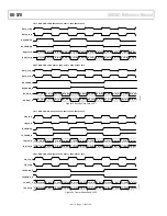
ENABLE
ENABLE is driven from the BBP to the
AD9361
to provide data
transfer burst control (along with TXNRX) in TDD mode.
ENABLE is asserted by the BBP for a minimum of a single
DATA_CLK cycle to indicate the start of each burst. It is
subsequently asserted a second time for a minimum of a single
DATA_CLK cycle to indicate the end of each burst.
The
AD9361
internally tracks the sequence of ENABLE pulses
to interpret each pulse correctly as either the start or finish of
each burst. The ENABLE signal can also be configured in level
mode, in which the state of the signal (not pulses) determines
when the ENSM moves between states. In LVDS mode, the data
ports are always active. In TDD mode, both the BBP and the
AD9361
ignore data in the inactive direction. The start and
finish latencies (between the ENABLE pulses being sampled by
the
AD9361
and the presence of the first and last valid data
samples on the bus) vary depending on data path configuration.
The Rx_FRAME and Tx_FRAME signals are used to determine
valid data by the BBP and the
AD9361
, respectively. The
FB_CLK signal is used to sample this input.
In FDD mode, the ENABLE signal serves as the single control
input to determine the state of the ENSM. There is also an
alternative FDD mode in which the ENABLE signal can be
redefined as RxON, a direct hardware control input to the
ENSM that controls the Rx function. In this mode (called FDD
independent control mode), the BBP independently controls
the Rx function, which can result in power consumption
savings.
Rev. A


