


UG-570
AD9361 Reference Manual
| Page 120 of 128
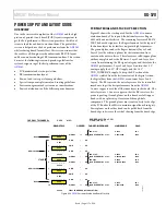
COMPONENT PLACEMENT AND ROUTING
GUIDELINES
The
AD9361
transceiver requires few external components to
function, but there are certain external components that are
critical to the proper functioning of the part. This section
provides a checklist for properly placing and routing some of
those critical signals and components.
•
The receiver/transmitter baluns and the matching circuits
affect the overall RF performance of the
AD9361
.
Therefore, every effort must be taken to optimize the
component selection and placement. Refer to the RF Port
Interface section for more information.
•
Pull the TEST/ENABLE ball (C4) to ground for proper
functioning. If this ball is not grounded then the
AD9361
will not function.
•
Pull the RESETB ball (K5) high with a 10 kΩ resistor to
VDD_INTERFACE for proper functioning. To reset the
part, pull the RESETB ball low.
•
Connect a 14.3 kΩ resistor to the RBIAS ball (L4). This
resistor must have a 1% tolerance.
•
If using an external clock, then connect the clock to the
XTALN ball (M12) via an AC coupling capacitor. (The
XTALP ball is a no connect in this case.) Ensure that the
external clock peak-to-peak amplitude does not exceed
1.3 V.
•
The Rx and the Tx external LO balls on the
AD9361
are
internally DC-biased. If these balls are used, connect a
series coupling capacitor to the ball. If the Rx and Tx
external LO balls are not used then connect them to
ground.
•
1 Ω resistor in series to the bypass capacitor on the
TX_VCO_LDO_OUT (B11) and RX_VCO_LDO_OUT
(G2) is needed. A capacitor that has a 1 Ω ESR can replace
this series combination of a resistor and capacitor.
•
The VDDA1P1_TX_VCO (A11) must be shorted to the
TX_VCO_LDO_OUT (B11) ball only.
•
The VDDA1P1_RX_VCO (G3) must be shorted to
RX_VCO_LDO_OUT(G2) ball only.
•
The Tx monitor balls also require a matching network. If
the Tx monitor is not used, then connect Ball A5 and Ball
M5 to ground. For more information, refer to the Tx Power
Monitor section.
•
There needs to be at least a 0.1 µF bypass capacitor near
each power supply ball.
•
Install 10 µF bypass capacitor on the VDDA1P3_RX_SYNTH
(J3) and VDDA1P3_TX_SYNTH (K3) ball.
•
Install a 10 µF capacitor near the Tx balun DC feed.
POWER MANAGEMENT AND SYSTEM NOISE
CONSIDERATIONS
The
AD9361
has three different power domains on the chip.
1.3 V is the main power domain that powers the major part of
the chip. The VDD_INTERFACE supply is a separate power
domain. The input voltage on the VDD_INTERFACE can range
from 1.2 V to 2.5 V. This voltage controls the voltage levels of
the digital interface of the
AD9361
. To operate the digital
interface in LVDS mode, supply 1.8 V or 2.5 V to the
VDD_INTERFACE supply. The input voltage to VDD_GPO
ball can range from 1.3 V to 3.3 V. The VDD_GPO must rise as
fast or faster than the 1.3 V supply domain.
All the different power domains have different power supply
noise rejection characteristics (PSRR). There are certain
supplies on the part that are more sensitive to noise than others
are. These supplies must be decoupled properly to achieve the
best performance from the
AD9361
. The noise considerations
for the 1.3 V analog supply are vital whereas the noise
considerations for the VDD_INTERFACE supply and the
VDD_GPO are less critical.
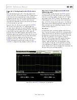
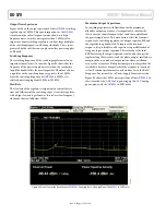
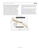
Table 54 lists the Rx EVM and Tx EVM degradation when a
ripple voltage is injected on the 1.3 V analog supply. In this
experiment, the LO was set to 700 MHz and the reference clock
was at 19.2 MHz with the RF PLL doubled. The Tx attenuation
setting was set to 10 dB. In this experiment, ripple voltage is
added on the 1.3 V DC supply with the help of a bias tee. This
combination powers all the 1.3 V analog supply domains. The
lower frequency ripple is more detrimental to the device
performance. For this reason, the low frequency noise must be
reduced on the platform that integrates the
AD9361
.
Table 54. 1.3 V Analog Supply Noise Sensitivities
Noise Frequency
Ripple Voltage
Rx EVM (10 MHz LTE)
Tx EVM (10 MHz LTE)
N/A
0 mV
−37.782 dB
−37.462 dB
40 KHz
16 mV
−24.886 dB
−28.619 dB
300 KHz
22 mV
−35.254 dB
−35.517 dB
500 KHz
52 mV
−36.254 dB
−35.517 dB
1 MHz
>50 mV
−37.501 dB
−36.95 dB
5 MHz
>50 mV
−37.749 dB
−36.927 dB
Rev. A


