


UG-570
AD9361 Reference Manual
Rev. A | Page 108 of 128
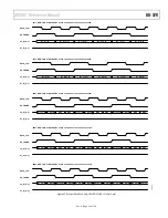
TXNRX
TXNRX is driven from the BBP to the
AD9361
and provides
data transfer burst control (along with ENABLE) when the
ENSM is in TDD mode. When ENABLE is sampled high by the
AD9361
to start a burst, the level on TXNRX is also sampled to
determine the data direction. In TDD mode, TXNRX sampled
high indicates a transmit burst and TXNRX sampled low
indicates a receive burst.
The TXNRX signal level must be maintained throughout a data
transfer burst (a valid logic level). The TXNRX signal may be
established any number of cycles (≥ 0) before the ENABLE start
pulse is sampled, and it may be changed any number of cycles
(≥ 0) after the ENABLE finish pulse is sampled. It is important
to note that the TXNRX signal should only change state while
the ENSM is in the ALERT state because the TXNRX rising and
falling edges power-up and power-down the corresponding
synthesizers directly in TDD mode.
In normal FDD mode, the TXNRX signal is ignored but must
be held at a valid logic level. There is also an alternative FDD
mode in which the TXNRX signal can be redefined as TxON, a
direct hardware control input to the ENSM that controls the Tx
function. In this mode (called FDD independent control mode),
the BBP independently controls the Tx function, which can
result in power consumption savings.
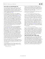
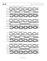
LVDS MAXIMUM CLOCK RATES AND SIGNAL
BANDWIDTHS
The data listed in Table 50 compares the maximum data clock
rates and signal bandwidths in the different allowable operating
modes for the LVDS data bus configuration. Maximum RF band-
widths are listed for two cases: sampling using the minimum
sample rate that avoids aliasing, and sampling using 2× over-
sampling. Details of each mode are given in subsequent sections.
The maximum DATA_CLK rate is increased to 245.76 MHz in
LVDS mode. This clock and the 56 MHz maximum analog filter
bandwidth limit RF channel signal bandwidth. Note that the
data bus timing is identical for TDD and FDD modes because
each path (transmit and receive) has a dedicated bus.
Table 50. Maximum LVDS Data Rates and Signal Bandwidths
Operating Mode
1R1T Configurations
1R2T/2R1T/2R2T Configurations
Maximum Data Rate -
Combined I and Q
Words (MSPS)
Maximum RF Channel Signal
Bandwidth (MHz)
Maximum Data
Rate—Combined I
and Q Words
Maximum RF Channel Signal
Bandwidth (MHz) per Channel
Using Minimum
Sample
Frequency
Using 2×
Oversampling
Using Minimum
Sample
Frequency
Using 2×
Oversampling
Dual Port Full Duplex
61.44
56
1
56
1
61.44
56
1
30.72
1
Limited by the analog filter bandwidth.


