


UG-570
AD9361 Reference Manual
| Page 114 of 128
[D11:D10]—
Bits[11:10] of the instruction word are unused.
[D9:D0]—
Bits[9:0] specify the starting byte address for the data
transfer during Phase 2 of the IO operation.
All byte addresses, both starting and internally generated
addresses, are assumed to be valid. That is, if an invalid address
(undefined register) is accessed, the IO operation continues as if
the address space were valid. For write operations, the written
bits are discarded, and read operations result in logic zeros at
the output.
Single-Byte Data Transfer
When NB2, NB1, and NB0 are all zero, a single-byte data
transfer is selected. In this scenario, the next eight bits to follow
the address bits contain the data being written to or read from
the
AD9361
register. Once the final bit is transferred, the data
signals return to their idle states and the SPI_ENB signal goes
high to end the communication session.
Multi-Byte Data Transfer
When NB2, NB1, and NB0 are all nonzero, a multibyte data
transfer is selected. The format and ordering of the data to be
transferred in this mode depend on whether the device is
configured for LSB-first or MSB-first data transfer.
For multibyte data transfers in LSB mode, the user writes an
instruction byte that includes the register address of the least
significant byte. The SPI internal byte address generator incre-
ments for each byte required in the multibyte communication
cycle. Data is written in least to most significant order as the
byte addresses are also generated in least to most significant
order.
For multi-byte data transfers in MSB mode, the user writes an
instruction word that includes the register address of the most
significant byte. The serial port internal byte address generator
decrements for each byte required by the multibyte commu-
nication cycle. Data is written in most to least significant order
as the byte addresses are generated in most to least significant
order.
Example
:
MSB-First Multibyte Transfer
To complete a 4-byte write, starting at Register 0x02A in MSB
first format, apply an instruction word of 1_011_000000101010
(binary). This instruction directs the
AD9361
SPI controller to
perform a write transfer of four bytes with the starting byte
address of 0x02A. After the first data byte is written, the
internal byte address generation logic decrements to 0x029,
which is the destination of the second byte. After the second
byte is written, the internal byte address generation logic
decrements to 0x028, which is the destination of the third byte.
After the third byte is written, the internal byte address
generation logic decrements to 0x027, which is the destination
of the last byte. After the fourth byte is written, the IO
communication cycle is complete and the next 16 falling clock
cycles on SPI_CLK are utilized to clock in the next instruction
word. If no further communication is needed, the data signals
return to their idle states, SPI_CLK goes low, and the SPI_ENB
signal goes high to end the communication session.
Example
:
LSB-First Multibyte Transfer
To complete a 4-byte write, starting at register 0x02A in LSB
first format, apply an instruction word of 010101000000_110_1
(binary). This instruction directs the
AD9361
SPI controller to
perform a write transfer of four bytes with the starting byte
address of 0x02A. After the first data byte is written, the
internal byte address generation logic increments to 0x02B,
which is the destination of the second byte. After the second
byte is written, the internal byte address generation logic
increments to 0x02C, which is the destination of the third byte.
After the third byte is written, the internal byte address
generation logic increments to 0x02D, which is the destination
of the last byte. After the fourth byte is written, the IO
communication cycle is complete and the next 16 falling clock
cycles on SPI_CLK are utilized to clock in the next instruction
word. If no further communication is needed, the data signals
return to their idle states, SPI_CLK goes low, and the SPI_ENB
signal goes high to end the communication session.
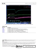
Timing Diagrams
The following diagrams in Figure 82 and Figure 83 detail the
SPI bus waveforms for a single-register write operation and a
single-register read operation, respectively. In the first figure,
the value 0x55 is written to Register 0x15A. In the second value,
Register 0x15A is read and the value returned by the device is
0x55. If the same operations were performed with a 3-wire bus,
the SPI_DO line in Figure 82 would be eliminated, and the
SPI_DI and SPI_DO lines in Figure 83 would be combined on
the SPI_DI line.
Rev. A


