


AD9361 Reference Manual
UG-570
| Page 119 of 128
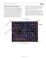
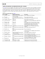
FAN-OUT AND TRACE SPACE GUIDELINES
The
AD9361
is in a 10 mm × 10 mm 144-pin BGA package.
The pitch between the balls is 0.8 mm. This small pitch makes it
impractical to route all signals on a single layer. RF balls are on
the outer edges of the
AD9361
package. This helps in routing
the critical signals without a fan-out via. The digital signals are
buried in the inner layers of the board. The digital balls
corresponding to the Rx data port are buried on one signal layer
and those corresponding to the Tx data port are buried on a
different signal layer. The
AD9361
evaluation boards use a
10-mil pin escape trace from the BGA land pad and drop the
digital signals on the inner layers by using a 6 mil via with a
12 mil keep out. The spacing between the BGA lands to the pin
escape via is 22 mils. Once the signal is on the inner layers, a
4.9 mil trace (50 Ω) connects the signal to the FPGA. The
recommended BGA land size is 14 mills.
Only one signal trace is routed between adjacent BGA land
pads and between pin escape vias on the inner layers. Routing
two traces between adjacent BGA land pads and pin escape vias
by reducing the BGA land pad width and trace-pad space
design rules reduces overall board manufacturing and assembly
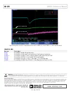
reliability. Figure 87 shows the fan out scheme evaluation board.
Figure 87. 0.8 mm Pitch BGA Via Fan-Out
22mi
l L
AND T
O
V
IA S
P
ACI
NG
10mi
l P
IN E
S
CAP
E
T
RACE
4.9mil TRACE (50
Ω)
Ø6mil PAD/12mil KEEP OUT
Ø14mil BGA
LAND SIZE
1
1668-
088
Rev. A


