


AD9361 Reference Manual
UG-570
| Page 117 of 128
POWER SUPPLY AND LAYOUT GUIDE
OVERVIEW
Due to the increased complexity of the
AD9361
and the high
pin count, printed circuit board (PCB) layout is important to
get the best performance. This section provides a checklist of
issues to look for and how to work on them. The goal of this
section is help achieve the best performance from the
AD9361
while reducing board layout effort. This section assumes that
the reader is a RF engineer who understands RF PCB layout
and has an understanding of RF transmission lines. This section
discusses the following issues and provides guidelines for
system designers to get the best performance out of the
AD9361
.
•
PCB material and stack up selection
•
RF transmission line layout
•
Fan-out and trace-space layout guidelines
•
Special components placement and routing guidelines
•
Power management and system noise considerations
•
Power distribution to all the different power domains
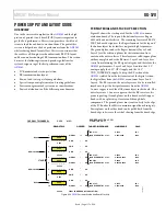
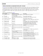
PCB MATERIAL AND STACK UP SELECTION
Figure 85 shows the stack up used for the
AD9361
customer
evaluation boards. The top and the bottom layers are Rogers
4003 with an 8 mil dielectric. The remaining layers are FR4-370
HR. The board design uses the Rogers laminate for the top and
the bottom layers for its low loss tangent at high frequencies.
The ground planes under the Rogers laminate (Layer 2 and
Layer 9) are the reference planes for the transmission lines
routed on the outer surfaces. These layers are solid copper plane
without any splits under the RF traces. Layer 2 and Layer 9 are
crucial to maintaining the RF signal integrity and, therefore, the
AD9361
performance. Layer 3 and Layer 8 contain the 1.3 V
analog supply, the 3.3 V GPO supply, and the 1.8 V
VDD_INTERFACE supply. To keep the RF section of the
AD9361
isolated from the fast transients of the digital section,
the digital lines from the
AD9361
are on inner Layer 5 and
Layer 6. The RF traces on the outer layers need to be controlled
impedance to get the best performance from the
AD9361
.
1 ounce copper is used for all the inner layers in this board. The
outer layers use 1.5 ounce copper so that the RF traces are less
prone to pealing. Ground planes on this board are full copper
floods with no splits except for vias and through-hole
components. The ground planes must route entirely to the edge
of the PCB under the SMAs to maintain signal launch integrity.
Power planes on the other hand can be pulled back from the
board edge to decrease the risk of shorting from the board edge.
Figure 85.
AD9361
Customer Evaluation Board Stack Up
0.008
0.003
0.008
0.008
0.003
SIGNAL
GND
PWR
PWR
SIGNAL
SIGNAL
SIGNAL
GND
GND
GND
1
2
3
4
5
6
7
8
9
10
1.5
1
1
1
1
1
1
1
1
0.003
0.003
0.0046
0.0046
OVERALL THICKNESS =
0.062
DIELECTRIC
COPPER
TARGET IMPEDANCE
LINE/SPACE
CALC
OZ
OZ
OZ
OZ
OZ
OZ
OZ
OZ
OZ
OZ
1.5
0.0606
FINAL THICKNESS (AFTER PLATING)
R4003
NEW LAYER
NEW LAYER
R4003
370 HR
50.1
100.0
50.0
100.2
50.0
100.2
ROGERS 4003 (DK = 3.38)
370 HR (DK = 4.1)
0.0155
0.008/0.006
0.008/0.006
0.0155
0.0038/0.0062
0.0038/0.0062
0.0049
0.0049
50Ω ± 10%
50Ω ± 10%
50Ω ±10%
50Ω ± 10%
100 DIFFERENTIAL ± 10%
100 DIFFERENTIAL ± 10%
100 DIFFERENTIAL ± 10%
100 DIFFERENTIAL ± 10%
±10%
50.1
100.0
1
1668-
086
Rev. A


