


your position is our focus
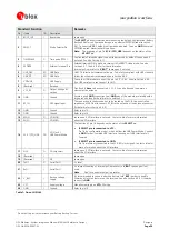
Function
PIN
(TIM)
I/O
Description
Remarks
Antenna
RF_IN
17
I
from
antenna
connector
(for
det
GPS
signal
input
The
connection
to
the
antenna
has
to
be
routed
on
the
PCB.
Use
a
controlled
impedance
of
50
Ohm
to
connect
RF_IN
to
the
antenna
or
the
antenna
ails
refer
to
Section 3.6.5)
Use
V_ANT
pin
to
supply
power.
Don’t
supply
DC
through
this
pin.
Connect
to
GND
if
Passive
Anten
V_ANT
19
I
Antenna
Bias
voltage
If
an
active
Antenna
is
used,
add
a
10R
resistor
(see
4.3.3.2
)
in
front
of
V_ANT
input
to
the
Antenna
Bias
Voltage
or
VCC_RF
for
short
the
antenna
supervisor
circuitry
(see
4.3.3.2
).
na
is
used.
circuit
protection
or
use
VC _RF
20
O
Output
Voltage
RF
V_ANT
).
The
max
power
consumption
of
the
Antenna
datasheet
specification
of
the
module
(see
also
4.3.3
).
C
Can
be
used
to
power
an
external
active
antenna
(
VCC_RF
connected
to
must
not
exceed
the
section
Leave
open
if
not
used.
AADET_N
27
I
Detect
Leave
open
if
not
used.
Active
Antenna
Signal
pin
for
optional
antenna
supervisor
circuitry
(
see 4.3.3.2
).
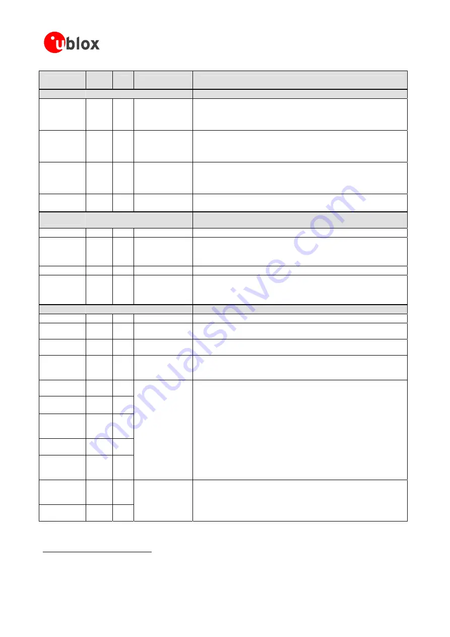
Serial Port
The
serial
interface
is
3V
CMOS
and
5V
TTL
compatible.
For
other
voltage
levels
use
the
appropriate
level
shifters.
TxD1
5
O
Serial
Port
1
3V
RxD1
4
I
Serial
Port
1
5V
tolerant
serial
port
input.
Internal
pull-up
resistor
to
V_BAT
.
Leave
open
if
not
used.
Note
Don’t
use
an
external
pull
up
resistor.
TxD2
6
O
Serial
Port
2
3V
RxD2
7
I
Serial
Port
2
5V
tolerant
serial
port
input.
Internal
pull-up
resistor
to
V_BAT
.
Leave
open
if
not
used.
Note
Don’t
use
an
external
pull
up
resistor.
System
BOOT_INT
3
I
Boot
mode
Do
not
connect
on
TIM-4A
and
TIM-4S
receivers.
RESET_N
22
I
Hardware
Reset
(Active
Low)
Leave
open
if
not
used.
Do
not
drive
high.
See
also
Section 4.9.2
.
TIMEPULSE
29
O
Timepulse
Signal
Configurable
Timepulse
signal
(one
pulse
per
second
by
default).
Leave
open
if
not
used.
See
also
Section 4.7.1
.
EXTINT0
23
I
External
Interrupt
External
Interrupt
Pin
to
wake
up
receiver
in
FixNOW™
sleep
mode.
See
also
Section 4.2.7.1
and
4.9.4
for
further
information.
Internal
pull-up
resistor
to
V_BAT
Leave
open
if
not
used.
GPSMODE2
PCS1_N/ P27
24
I/O
GPSMODE5/
SCK1/ P17
8
I/O
GPSMODE6/
SS_N/ P26
PCS0_N/
25
I/O
GPSMODE12/
30
I/O
PCS3_N/ P29
GPSMODE3/
EXTINT1/
P13/
9
I/O
GPSMODE
Pin
TIM-4A/ TIM-4S:
GPSMODE
Pin;
leave
open
if
default
configuration
is
used.
Refer
to
Section
4.8.2
for
fur
r
information.
TIM-4H / TIM-4P:
GPIO
Pin;
leave
open
if
not
used.
The
General
Purpose
I/O
(GPIO)
can
only
be
programmed
with
the
ANTARIS
®
4
Software
Customization
Kit,
please
refer
to
the
SCK Manual [8]
when
intending
to
use
of
the
GPIO’s
of
the
receiver.
GPIO/
the
NU / SCK/
P23
26
I/O
NU/ MOSI/
P24/
28
I/O
GPIO
/
NC
TIM-4A/ TIM-4S:
Not
connected;
leave
open.
TIM-4H / TIM-4P:
GPIO
Pin;
leave
open
if
not
used
Table 6: Pin-out TIM-4x
5
Do
not
pull
up
as
it
may
increase
your
Battery
Backup
Current.
6
Pull
to
GND
to
achieve
Normal
Sensitivity
Mode
setting
at
startup.
GPS
Modules
-
System
Integration
Manual
(SIM)
(incl.
Reference
Design)
Design-In
GPS.G4-MS4-05007-A1
Page 48