


your position is our focus
C Demo Design
C.1 TIM - GPS standalone Receiver
C .1
tic
Pl
se
refer
to
Sectio
implement
ual
for
your
GP
receiver.
C .2
of Ma
There
addition
onents
ne
design
ARIS
®
GP
the
optional
active
antenna
supervisor
circuitry
is
then
refe
ction 4.3
C.1.3 Layout
Figure
igu
exam
app
ard
based
on
u-blox
PS2
board.
One
can
easily
identi
e
nu
d
the
ground
a
top
l
k
(1.6
m
mi
quite
wide.
Unfortu
mount
the
upper
left
corner
required
a
n
ro
easur
how
s
no
slot
in
the
groun
on
the
r
at
th
helps
the
no
input.
This
w
necessary
in
this
design
because
the
RF
connector
sits
quite
close
to
the
digital
I/Os
of
the
receiver.
If
in
a
different
design,
the
ector
could
b
ved
furth
,
the
slot
would
likely
not
be
necessary
and
a
layout
similar
to
Figure 43
will
work
fine.
Increasing
the
length
of
this
slot
is
not
recommended
and
will
not
further
im o
ormance
.1
Schema
ea
n 3
to
your
individ
needs
S
standalone
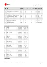
.1 Bill
terial
is
not
al
comp
eded
to
an
ANT
S
receiver.
If
required
r
to
Se
.
118
and
F
re 119
show
ples
of
an
lication
bo
fy
the
larg
m)
also
the
mber
of
vias
an
cro
strip
gets
reas
on
the
nately,
the
ayer.
Since
the
dielectric
is
rather
thic
ing
hole
in
tre ch
in
the
mic
d
plane
strip
line.
M
bottom
laye
ements
s
e
left
end
that
this
ha
to
isolate
significant
effect.
The
small
isy
digital
part
from
the
RF
as
conn
e
mo
er
up
pr ve
perf
.
Figure 118: Reference la
r on 2-l
m FR-
yout: Top laye
ayer 1.6 m
4 material
GPS
Modules
-
System
Integration
Manual
(SIM)
(incl.
Reference
Design)
Demo
Design
GPS.G4-MS4-05007-A1
Page 162