your position is our focus
LEA-LA
LEA-4A / LEA -4S
Remarks for Migration
Pin
Pin
Name
Typical
Assignment
Pin
Name
Typical
Assignment
22 GPSMODE2
Connected
to
GND
or
VDD_18OUT
GPSMODE2/
GPSMODE23
Not
connected
Backward
compatible:
This
pin
can
be
connected
to
GND,
VDD18OUT
or
VCC.
An
external
pull
up
resistor
is
not
required
as
there
is
one
built-in.
23 NC
Not
connected
GPSMODE7
Not
connected
24 NC
Connected
to
GND
VDDUSB
Connected
to
GND
25 NC
Not
connected
USB_DM
Not
connected
26 NC
Not
connected
USB_DP
Not
connected
Placing
a
LEA-4x
into
an
existing
LEA-LA
board
design
will
disable
USB
port.
27 EXTINT0
Connected
to
VDD18OUT
EXTINT0
Not
connected
Do
not
add
an
external
pull
up
resistor;
there
is
one
built-in
to
V_BAT
.
Leave
open
if
not
used.
28 TIMEPULSE
1.8V
out
TIMEPULSE
VDDIO
level
I/O
Consider
that
TIMPULSE
on
LEA-4x
is
on
VDDIO
voltage
level
(1.8V
on
LEA-LA)
J
:
Pins
to
be
checked
carefully
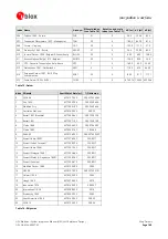
Table 79: Pin-out comparison LEA-LA vs. LEA-4A/4S
D.3 Migration from LEA-LA to LEA-4H/LEA-4P
The
pin-outs
of
LEA-LA
and
LEA-4H/4P
differ
slightly.
compares
the
modules
and
highlights
the
differences
to
be
considered.
Table 80
LEA-LA
LEA-4H / LEA-4P
Remarks for Migration
Pin
Pin
Name
Typical
Assignment
Pin
Name
Typical
Assignment
1 TXD2
VDDIO
level
I/O
MISO
VDDIO
level
I/O;
not
connected
2 RXD2
VDDIO
level
I/O;
pull
up
if
not
used
MOSI
VDDIO
level
I/O;
not
connected
Serial
Port
2
not
supported
on
LEA-4P/LEA-4H.
Leave
open
if
not
used.
3 TXD1
VDDIO
level
I/O
TXD1
VDDIO
level
I/O
No
difference
4 RXD1
VDDIO
level
I/O;
pull
up
if
not
used
RXD1
VDDIO
level
I/O
Do
not
add
an
external
pull
up
resistor;
there
is
one
built-in
to
V_BAT
.
Leave
open
if
not
used.
5 VDDIO
1.65
–
3.60V
VDDIO
1.65
–
3.60V
To
be
compatible
to
LEA-LA,
VDDIO
has
to
be
set
to
Vcc
to
assure
a
3.0V
level
at
the
serial
ports.
The
GPSMODE
pins
do
recognize
1.8V
and
3.0V
as
“high”
value
at
VDDIO
.
6 VCC
2.70
–
3.30V
VCC
2.70
–
3.30V
No
difference
7 GND
GND
GND
GND
No
difference
8 VDD18OUT
Not
connected
VDD18OUT
Not
connected
No
difference
9 GPSMODE6
Connected
to
GND
or
VDD_18OUT
PCS0_N
Not
connected
Backward
compatible:
can
be
left
open
or
connected
to
GND,
VDDIO
or
VDD_18OUT.
10 RESET_N
1.8V
RESET_N
1.8V
No
difference
(see
Section
4.9.2).
11 V_BAT
1.95
–
3.6V
V_BAT
1.50
Wider
voltage
range.
Uncritical
for
migration.
–
3.6V
12 BOOT_INT
NC
BOOT_INT
NC
No
difference
13 GND
GND
GND
GND
No
difference
14 GND
GND
GND
GND
No
difference
15 G
fference
ND
GND
GND
GND
No
di
16 RF_IN
RF_IN
RF_IN
RF_IN
No
difference
17 GND
GND
GND
GND
No
difference
18 VCC_RF
VCC
-
0.1V
VCC_RF
VCC
-
0.1V
No
difference
19 V_ANT
3.0V
–5.0V
V_ANT
3.0V
-5.0V
No
difference
20 AADET_N
Connected
to
GND
AADET_N
Not
connected
No
external
pull
down
resistor
required,
as
there
is
already
an
internal
pull
down
resistor.
Please
check
resistor
values
in
Section 4.3.3.2.
21 GPSMODE5
Connected
to
GND
or
VDD_18OUT
EXTINT1
Not
connected
Do
not
add
an
external
pull
up
resistor;
there
is
one
built-in.
Leave
open
if
not
used.
If
permanently
connected
to
GND,
the
FixNOW
sleep
25
Connecting
the
GPSMODE23
pin
(LEA-4S)
to
GND
increased
the
FixNOW
sleep
mode
current
by
about
50µA.
Connecting
the
GPSMODE2
pin
(LEA-4A)
to
GND
does
however
not
have
an
impact
on
the
FixNOW
sleep
mode
current.
GPS
Modules
-
System
Integration
Manual
(SIM)
(incl.
Reference
Design)
Migration
to
ANTARISP®P4
receivers
GPS.G4-MS4-05007-A1
Page 168

