


your position is our focus
D.4 Migration
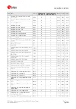
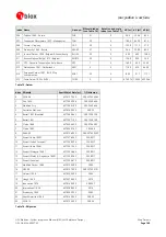
The
pin-outs
of
TIM
from TIM-Lx to TIM-4x pin out
-Lx
and
TIM-4x
modules
do
not
differ
significantly.
Table 81
compares
the
modules
and
ighlights
the
differences
to
be
considered.
Please
note
that
this
table
does
not
consider
any
migration
from
TIM-LR.
h
TIM-Lx
TIM-4x
Remarks
Pin
Pin
Name
Typical
Assignment
Pin
Name
Typical
Assignment
1 VCC
2.70
–
3.30V
VCC
2.70
–
3.30V
No
difference
2 GND
GND
GND
GND
rence
No
diffe
3 BOOT_INT
NC
BOOT_INT
NC
rence
No
diffe
4 RXD1
3.0V
in;
pull
up
to
VCC
if
not
used
RXD1
1.8
-
5.0V
in
Do
not
add
an
external
pull
up
resistor;
there
is
one
built-in
to
V_BAT
.
Leave
open
if
not
used.
5 TXD1
3.0V
out
TXD1
3.0V
out
No
difference
6 TXD2
3.0V
out
TXD2
3.0V
out
No
difference
7 RXD2
3.0V
in;
pull
up
to
used
RXD2
1.8
-
5.
VCC
if
not
0V
in
Do
not
add
an
external
pull
up
resistor;
there
is
one
built-in
to
V_BAT
.
Leave
open
if
not
used.
8
P17 /
GPSMODE5
1.8V
I/O
(LP:
3.0V),
not
connected
P17/
GPSMODE5
3.0V
I/O
connected
nce
,
not
No
differe
9
GPSMOD
STATUS /
1.8V
I/O
(LP
E3
:
3.0V),
not
connected
EXTINT1 /
GPSMODE3
3.0V
I/O,
connecte
not
d
Status
Pin
not
available
anymore;
No
difference
otherwise.
10
VDD18_OUT /
TIM-LP:
NC/GND
Not
connected
VDD18OUT
Not
connected
No
difference,
except
for
TIM-LP
.
11
to
16
GND
GND
GND
GND
No
difference
17 RF_IN
RF_IN
RF_IN
RF_IN
No
difference
GND
GND
GND
rence
18 GND
No
diffe
3.0V
-5.0V
V_ANT
3.0V
-5.0
No
difference
19 V_ANT
V
20 VCC_RF
VCC
-
0.1V
VCC_RF
VCC
-
0.1
No
difference
V
21 V_BAT
1.95
–
3.6V
V_BAT
1.50
–
Uncritical
for
migration.
3.6V
Wider
voltage
range.
22 RESET_N
1.8V
RESET_N
1.8V
No
difference.
Don’t
drive
high.
Refer
to
Section 4.9.2
for
more
information.
23 EXTINT0
Not
connected
EXTINT0
Not
con
No
difference
nected
PCS1_N/
GPSMODE2
difference
24
GPSMODE2
PCS1_N/
No
25
PCS0_N/
GPSMODE6
PCS0_N/
GPSMODE6
No
difference
E7
1.8V
I/O
(LP:
3.0V),
SCK/
NC
3.0V
I/O,
not
connected
No
difference
on
Programmable
receivers.
But
on
TIM-4A:
the
Navigation
rate
cannot
be
changed
anymore.
It’s
always
1Hz.
26
SCK/
GPSMOD
not
connected
No
external
pull
down
resistor
required
as
there
27 AADET_N
Not
connected
AADET_N
Not
connected
is
already
an
internal
pull
down
register.
Please
check
resistor
values
in
Section 4.3.3.2
.
28
GPSMODE8
MOSI/
1.8V
I/O
(LP:
3.0V),
MO
not
connected
SI/
P24
3.0V
I/O
connec
on
Programmable
receivers.
/
TIM-4S:
the
Navigation
rate
be
d
anymore.
It’s
always
1Hz.
,
not
rence
ted
But
on
TIM-4A
nnot
change
No
diffe
ca
1.8V
out
(LP:
3.0V)
TIMEPULSE
3.0V
ou
29 TIMEPULSE
t
Same
function
but
different
output
voltage.
30
PCS3_N/
GPSMODE12
1.8V
I/O
(LP:
3.0V),
not
connected
PCS3_N/
GPSMODE 12
3.0V
I/O,
not
connecte
No
difference
d
J
ns
to
be
checked
carefully
Pin-out comparison TIM-Lx vs. TIM-4x
:
Pi
Table 81:
is
only
significant
when
using
GPIO
pin
functionality
together
with
an
SCKit
application.
26
Higher
output
voltage
GPS
Modules
-
System
Integration
Manual
(SIM)
(incl.
Reference
Design)
Migration
to
ANTARISP®P4
receivers
GPS.G4-MS4-05007-A1
Page 170