


www.ti.com
6.2
PLL Configuration During Operation
6.3
PLL1, PLL2, and SRIO Reference Clock Solutions
6.3.1
Clock Requirement
6.3.2
CLKIN1/CLKIN2 Solutions
6.3.2.1
Single Device Solution
Clocking
The following process should be followed to change the PLL after it has been operating. The wait times
are conservative durations to guarantee proper operation.
1. Program PLLCTL.PLLENSRC=0 to enable the PLLTL.PLLEN bit.
2. Program PLLEN=0 (PLL bypass mode) and PLLRST=1 (reset PLL) in PLLCTL register.
3. Program PREDIV, PLLM for the desired multiplier and divider.
4. Wait for at least 256 CLKIN1 cycles for the PLL to reset.
5. Set PLLRST=0 to de-assert PLL reset.
6. Wait for 3000 CLKIN1 cycles for the PLL to lock.
7. Set PLLEN=1 to switch from Bypass mode to PLL mode.
This section describes the clock requirements and a system solution for the input clocks to the TCI6482
device that require special consideration. CLKIN1 is the reference clock to PLL1 which is used to generate
the core clock (up to 1GHz). This clock requires a low jitter clock source. CLKIN2 is the reference clock to
PLL2 which is used to generate the clock for the DDR2 and EMAC subsystems. This clock, when used as
the reference clock to the DDR2 subsystem, must be low jitter. The SRIO reference clock (RIOCLK,
RIOCLK) requires a differential low jitter clock source and proper termination.
It is also assumed that multiple TMS320TCI6482 devices may be used on a board so the proposed
system solutions include clock fanout buffers.
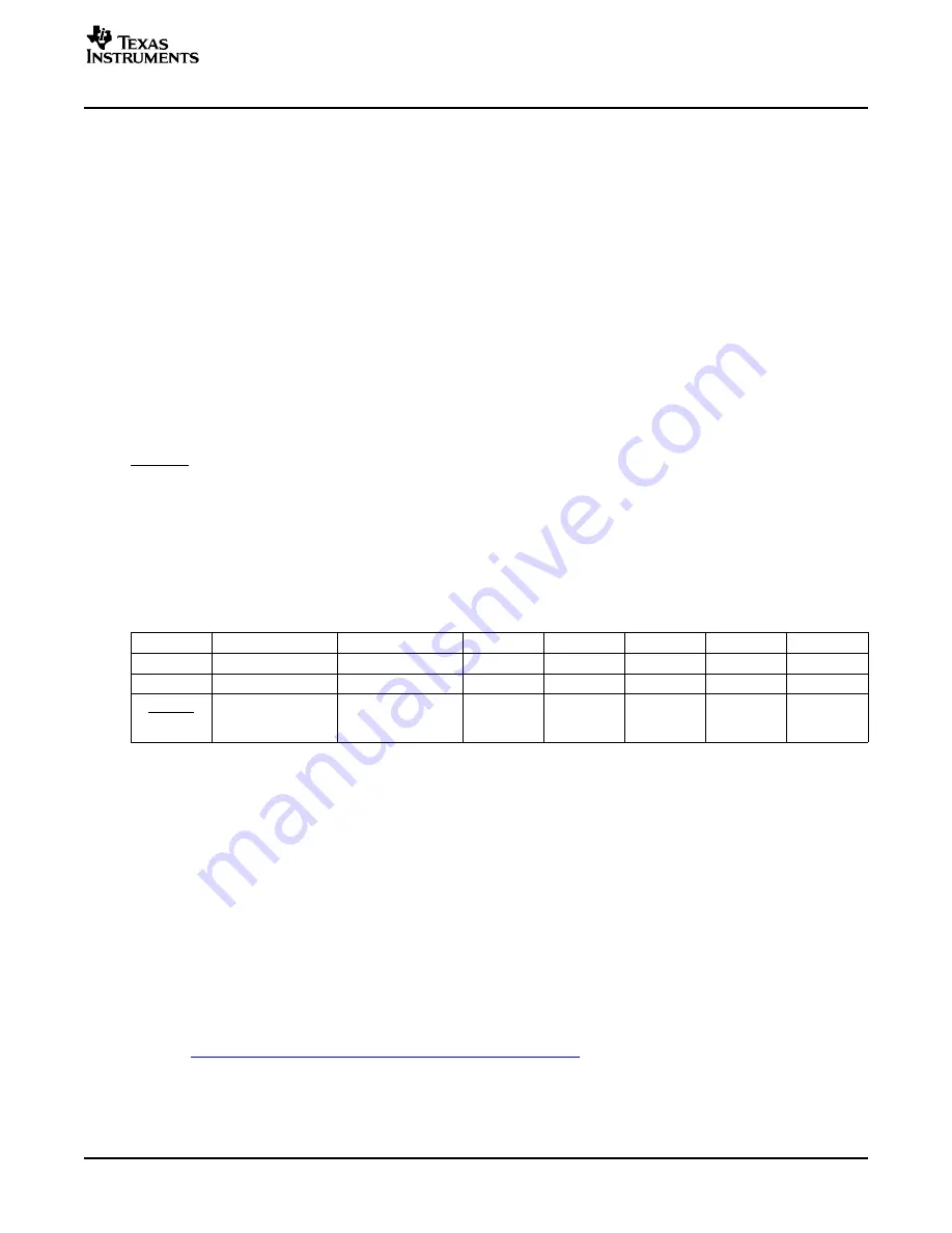
The clock requirements are given in
Table 5
.
Table 5. Reference Clock Requirements
Logic
Input Jitter
(1)
Trise/Tfall
Duty Cycle
Stability
Freq
(2)
PLL Freq
CLKIN1
LVCMOS or LVTTL
100pS pk-pk
Max 1.2nS
40/60%
50PPM
50MHz
1GHz
CLKIN2
LVCMOS or LVTTL
100pS pk-pk
Max 1.2nS
40/60%
50PPM
25MHz
250MHz
RIOCLK,
Differential LVDS or
4pS RMS
50pS -
45/55%
50PPM
125MHz,
3.125GHz
RIOCLK
LVPECL
56ps pk-pk @
700pS
156.25MHz
1x10E
-12
BER
(1)
Assumes a Gaussian distribution. Peak-peak jitter assumes 100,000 points.
(2)
Recommended operating frequencies based on component availability and supported PLL multipliers.
Trise/Tfall values are given for CLKIN1 and CLKIN2 transitions from 0.8V to 2.0V. This is equivalent to a
max Trise/Tfall of 2nS from 20% to 80% of 3.3V. RIOCLK Trise/Tfall values are given for 20% to 80% of
the voltage swing. These rise/fall times assume the maximum jitter values. Slower rise/fall times can be
used if the jitter is lower.
CLKIN1 and CLKIN2 have similar requirements for a clock source so the same clocking solutions (except
for frequency) can be used for both.
It is assumed that the source clock for each of these clocks is an oscillator on the same board as the
TMS320TCI6482. Use of distributed clocks may require a jitter cleaner device such as the CDCM7005
(refer to
http://focus.ti.com/docs/prod/folders/print/cdcm7005.html
). Most PLL based clock generators do
not meet the input jitter requirement. If an on-board oscillator is used with one TMS320TCI6482 no other
components should be needed except for termination resistors.
SPRAAC7B – April 2006
TMS320TCI6482 Design Guide and Migration from TMS320TCI100
9
Submit Documentation Feedback


