Texas Instruments TMS320TCI6482 Скачать руководство пользователя страница 20

www.ti.com

7.6.1

Selecting Bulk Capacitance

7.6.2

Recommended Capacitance

Power Supply

There are 2 factors that need to be considered when selecting the bulk capacitance: the effective ESR for
the power plane capacitors, and the amount of capacitance needed to provide power during periods when
the voltage regulator cannot respond.

The overall impedance of the core power plane is determined by:

(Allowable

Voltage

Deviation

due

to

Current

Transients)

/

(Max

Current)

In

Section 7.5

, it was suggested that the allowable voltage deviation allowed due to transient response is

18mV. The max transient current is estimated at 1.5A. So the impedance requirement is 18mV / 1.5Amps
= 12mohms. The power plane also has some impedance. An estimate of 2mohms will require a total
effective ESR of 10mohms. So the effective ESR of the bulk capacitors should not exceed this value.
Multiple bulk capacitors in parallel will help achieve this overall ESR.

The amount of the bulk capacitance is determined by the amount of time that the power regulator cannot
respond to the power demand and the amount of power that needs to be delivered during this time. The
maximum current change measurements have been made which show:

Max current swing: 1.5Amp

The decoupling caps provide the immediate current through the transition but the bulk capacitors need to
supply this current until the voltage regulator can respond. A typical power regulator would have about a
10KHz bandwidth with a large capacitive load (needed to maintain the 18mV deviation). Assuming this
bandwidth and a 1.5A current transient, the minimum bulk capacitance needed is estimated at 1500uF. So
for this case the bulk capacitance needs to add up to 1500uF and create an effective ESR of 10mohms.
The capacitance may need to be further increased to cover temperature derating. Examples of suitable
capacitors are shown in

Table 8

.

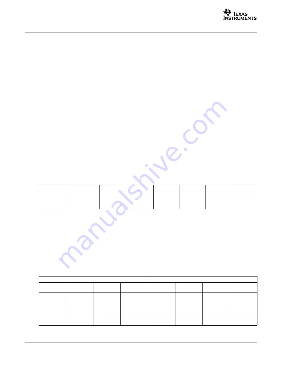
Table 8. Bulk Capacitor Examples

Manufacturer

Type

Part Number

C

Vmax

ESR

QTY

AVX

Tantalum

TPSD337K004R0035

330uF

4V

35m

5

KEMET

Tantalum

T530X687M004ASE005

680uF

4V

5m

3

SANYO

POS-CAP

2R5TPD1000M5

1000uF

2.5V

5m

2

Capacitor selection should be done as shown above for the specific power supply implementation. If
multiple TCI6482 devices are used on a single core power plane the total capacitance could be reduced
per device if the expectation was that the transients would not occur on all devices simultaneously.

Recommended capacitor selection is given in

Table 9

where it is also compared with the TCI100 capacitor

recommendations. The TCI6482 capacitor selection does not necessarily include power supply output
capacitance. Output capacitors are provided along with the power supply reference designs.

Table 9. Capacitor Recommendations

TCI6482

TCI100

Voltage

Capacitors

Total

Description

Voltage

Capacitors

Total

Description

Supply

Capacitance

Supply

Capacitance

CVDD

10 * 560pF

2084uF

1.2V Core

CVDD

1 * 330uF

333.2 uF

Core

20 * 100nF

32 * 100nF

3 * 680uF

2 * 22uF

DVDD33

16 * 560pF

330uF

3.3V I/O

DVDD

1 * 330uF

333.2 uF

I/O

24 * 100nF

32 * 100nF

1 * 330uF

20

TMS320TCI6482 Design Guide and Migration from TMS320TCI100

SPRAAC7B – April 2006

Submit Documentation Feedback

Содержание TMS320TCI6482

Страница 1: ...e Configurations and Initialization 6 6 Clocking 8 7 Power Supply 14 8 I O Buffers 21 9 Peripheral Section 22 Appendix A TCI6482 RGMII 1 5V 1 8V to 2 5V 3 3V Translation 40 List of Figures 1 CLKIN1 CLKIN2 Single Device Clock Solution 10 2 PLL1 PLL2 Multiple Device Clock Solution 11 3 RIOCLK Single Device LVDS Clock Solution 12 4 RIOCLK Multiple Devices LVDS Clock Solution 12 5 RIOCLK Multiple Devi...

Страница 2: ...5 13 PCI Comparison TCI6482 vs TCI100 26 14 McBSP Comparison TCI6482 vs TCI100 27 15 VCP2 Summary of Changes on TCI6482 28 16 VCP2 Usage Change on TCI6482 28 17 VCP2 Register Changes on TCI6482 29 18 TCP2 Summary of Changes on TCI6482 29 19 TCP2 Usage Change on TCI6482 30 20 TCP2 Register Changes on TCI6482 30 21 GPIO Interrupt Comparison TCI6482 vs TCI100 31 22 Timer Comparison TCI6482 vs TCI100 ...

Страница 3: ...ut Output GPIO User s Guide SPRU725 TMS320TCI648x DSP 64 Bit Timer User s Guide SPRU818 TMS320TCI648x DSP Enhanced DMA EDMA Controller User s Guide SPRU727 TCI6482 DSP Inter Integrated Circuit I C Module User s Guide SPRUE11 TMS320TCI648x DSP Ethernet Media Access Controller EMAC Management Data Input Output MDIO User s Guide SPRUE12 TMS320TCI648x DSP Universal Test and Operations PHY Interface fo...

Страница 4: ...1 selectable PCI 32 bit 1 PCI 32 bit 1 66 MHz or 33 MHz 33 MHz McBSP 2 McBSP 3 Internal clock source up to 90 MHz UTOPIA 8 bit mode 1 Same 50 MHz Slave only 10 100 1000 Ethernet 1 N A N A MAC EMAC Management Data 1 N A N A Input Output MDIO 64 bit Timers 2 64 bit or 32 bit Timer 3 32 bit timers Configurable 4 32 bit Internal clock source CPU Clock 6 External clock source up to CPU clock 24 VLYNQ 1...

Страница 5: ...h devices and through the JTAG ID register at address 0x02A80008 on the TCI6482 device Table 2 identifies the JTAG BSDL ID differences between the TCI100 and TCI6482 Table 2 TCI6482 and TCI100 JTAG BSDL IDs JTAG BSDL ID Device Variant 31 28 Part Number 27 12 Manufacturer 11 1 LSB TCI6482 xxxxb 1 0000000010001010b 00000010111b 1 0 TCI100 xxxxb 2 0000000010000001b 00000010111b 1 1 Variant field indi...

Страница 6: ...owns While POR is low large currents may be seen on the DVDD33 power plane due to floating inputs i e the EMIF bus If the user wishes to avoid these currents external pull ups or pull downs should be used Refer to the TCI6482 Silicon Errata document for complete details In revision 2 0 silicon and later the internal pull up and pull down resistors will not be disabled under any conditions The RESE...

Страница 7: ...s For details refer to the TMS320TCI6482 Bootloader User s Guide document The interfaces which support a boot loading process are I2C HPI PCI Serial RapidIO and EMIF 8 bit ROM In addition a first level boot loader loaded using one of those interfaces can configure the Ethernet or Utopia interfaces for a secondary boot load For a summary of the boot modes supported refer to the TCI6482 data manual ...

Страница 8: ...subsequent versions this PLL is not required for RMII operation The PLL1 controller powers up in bypass x1 mode with PLL1 in reset Some boot modes change this multiplier see Section 5 6 After the PLL1 is out of reset and running changing the PLL1 controller multiplier and divider values or the reference clock frequency involves using the PLL reset mode to clear the lock condition The PLL reset mod...

Страница 9: ... clock fanout buffers The clock requirements are given in Table 5 Table 5 Reference Clock Requirements Logic Input Jitter 1 Trise Tfall Duty Cycle Stability Freq 2 PLL Freq CLKIN1 LVCMOS or LVTTL 100pS pk pk Max 1 2nS 40 60 50PPM 50MHz 1GHz CLKIN2 LVCMOS or LVTTL 100pS pk pk Max 1 2nS 40 60 50PPM 25MHz 250MHz RIOCLK Differential LVDS or 4pS RMS 50pS 45 55 50PPM 125MHz 3 125GHz RIOCLK LVPECL 56ps p...

Страница 10: ... 2 1 can be used for the fan out case The oscillator output specifications should be compared to the fanout buffer input specifications to make sure they are compatible A low jitter fanout buffer is required which generally means a non PLL based fanout buffer should be used Suggested solutions for fanout buffers are TI CDCV304 1 4 Clock buffer http focus ti com lit ds symlink cscv304 pdf TI CDCVF2...

Страница 11: ...ane should be placed below the oscillator Digital signals should not be routed near or under the clock sources Maintain at least 25 mil spacing to other traces The SerialRapidIO reference clock requires special considerations because it is differential must be low jitter and requires termination Either an LVDS or LVPECL clock source can be used but they require different terminations The input buf...

Страница 12: ...nts for RIOCLK RIOCLK Figure 3 shows an LVDS based solution including terminations Figure 4 shows an LVPECL based solution including terminations The terminations shown are still being investigated and should be considered preliminary Figure 3 RIOCLK Single Device LVDS Clock Solution Figure 4 RIOCLK Multiple Devices LVDS Clock Solution For systems with multiple TMS320TCI6482 devices it may be pref...

Страница 13: ... clock output buffer the CDCL6010 can be used These buffers have not been tested but are examples of buffers that meet the specification requirements for RIOCLK RIOCLK Jitter performance for the SN65LVDS108 is found in its datasheet For the CDCLVP110 the jitter characteristics of these parts refer to CDCLVP110 Jitter Info http focus ti com lit an scaa068 scaa068 pdf Figure 5 shows a diagram of a s...

Страница 14: ...D15 DVDD12 PLL DDR2 SRIO SRIO DLL TCI6482 1 2V 3 3 3V 1 8V 1 5V 1 2V 1 8V 1 8V 1 2V or 1 8V TCI100 1 1V 3 3 3V N A N A N A 3 3V N A N A 1 2V 3 All power supplies may be generated from switching supplies with the exception of the SRIO 1 2V supplies DVDD12 AVDDA and AVDDT Due to the noise sensitivity of the SRIO SERDES links a linear regulator with proper filtering is recommended A switching regulat...

Страница 15: ...DDRM SRIO DVDD12 SRIO AVDDA SRIO AVDDT SRIO DVDD18 Required Optional TCI6482 voltage planes Power Supply Figure 7 Power Supply Generation Filters on AVDLL1 and AVDLL2 are not needed if the DDR2 interface is not used The recommended filter circuit from Figure 7 is given in Figure 8 The filter component shown is a from Murata part If a different part is cross referenced the frequency envelope must b...

Страница 16: ...e details on VREFSSTL can be found in Implementing DDR2 PCB Layout on the TMS320TCI6482 SPRAAA9 Note that if the RGMII interface is not used and is disabled VREFHSTL can be connected to directly to VSS Figure 9 Reference Voltage Generation The recommended power sequence is described in the TCI6482 data manual This is the sequence which is used for manufacturing device test Other sequences may work...

Страница 17: ...h clearance between this and any switching signals The filter circuits should be placed as close to the corresponding TCI6482 power supply pin s as possible No digital switching signals should be routed near or directly under the filter circuits The voltage tolerances specified in the datasheet include all DC tolerances and the transient response of the power supply These specify the absolute maxi...

Страница 18: ...ltage monitor DVDD18MON A26 Die side 1 8V DVDD18 voltage monitor DVDD15MON F3 Die side 1 5V or 1 8V DVDD15 voltage monitor These monitor pins should be connected directly to the positive side sense pin of the voltage regulator This may not be needed if the regulator used has a low impedance path between its VOUT and SENSE pins Since the voltage regulator output could become unstable and drive to a...

Страница 19: ...noise place as many capacitors caps as possible close to the DSP Assuming 0402 caps the user should be able to fit the number of capacitors given in Table 9 These caps need to be close to the DSP no more than 1 25 cm maximum distance to be effective Ideally these caps should be connected directly to the via attached to the BGA power pin Parasitic inductance limits the effectiveness of the decoupli...

Страница 20: ...capacitive load needed to maintain the 18mV deviation Assuming this bandwidth and a 1 5A current transient the minimum bulk capacitance needed is estimated at 1500uF So for this case the bulk capacitance needs to add up to 1500uF and create an effective ESR of 10mohms The capacitance may need to be further increased to cover temperature derating Examples of suitable capacitors are shown in Table 8...

Страница 21: ...set Some peripherals that are disabled via the reset configuration can have their dedicated power planes be connected to VSS This achieves the lowest possible power dissipation These peripherals are SRIO All SRIO power planes DVDDRM DVDDR DVDD12 AVDDA AVDDT connect to VSS RGMII DVDD15 VREFHSTL RSV07 RSV08 RSV13 RSV14 connected to VSS DDR2 VREFSSTL RSV11 RSV12 connect to VSS Connecting these interf...

Страница 22: ...exception of DDR and SRIO on a TCI6482 design be checked using IBIS simulations For more details on performing IBIS simulations see Using IBIS Models for Timing Analysis SPRA839 The clock for many peripherals is generated by a divide down from the CPU core clock Since the CPU core clock is different than the TCI100 the divider and timings should be checked This impacts the McBSP EMIFA and Timer Pe...

Страница 23: ...4 is CPU core clock 8 The SYSCLK4 divider can be changed via software register accesses to PLL1 If the EMIFA peripheral is not used most EMIFA inputs can be left unconnected Internal pull up and pull down resistors are included on this interface so leakage will be minimal Some EMIFA signals are used for boot stapping options that are latched on the rising edge of POR cold boot or rising edge of RE...

Страница 24: ...Ohms data and AECLKOUT 25 Ohms 50 Ohms control Documentation for HPI TMS320TCI648x DSP Host Port Interface HPI User s Guide SPRU874 TCI6482 System Boot TCI6482 IBIS Model File Using IBIS Modes for Timing Analysis SPRA839 The HPI interface is multiplexed with the PCI inteface Selection between HPI and PCI is done via boot strapping and latched by reset If HPI is selected a second boot strapping opt...

Страница 25: ...single PHY mode If PCI is selected a second boot strapping option allows the PCI to get auto initialized from an I2C ROM The PCI auto initialization table if used needs to be installed at offset 0x400 in the I2C ROM This allows Boot over I2C ROM and PCI auto initialization to both utilize the same EEPROM Another PCI strapping option selects between 33MHz and 66MHz PCI This needs to be strapped bas...

Страница 26: ...een McBSP1 and GPIO pins After a reset software must enable the McBSP interface s The McBSP module receives SYSCLK3 as its input clock which runs at the CPU core clock 6 The McBSP port clocks can either be driven by an external clock CLKS or by an internal clock which is derived from SYSCLK3 There is only one CLKS input which supplies both McBSP ports but both ports can individually be programmed ...

Страница 27: ...600ohms 03 trace 03 trace 9 4 3 TCI6482 McBSP vs TCI100 McBSP 9 5 Enhanced VCP 9 5 1 Configuration of VCP2 Peripheral Section TI performed simulations on an 8 TCI6482 topology and the best routing topology for this is shown in Figure 12 This topology was able to operate with a 10MHz McBSP clock Figure 12 McBSP 8 Load Routing Topology All the same McBSP modes are available on the TCI6482 as the TCI...

Страница 28: ...ws in soft decision mode Output FIFO RAM 32 x 64 64 x 64 Soft Decision Resolution 12 bits 8 bits Hard Decision Ordering Oldest bit is in the MSB Programmable More flexibility Debugging Features Pause Pause after each sliding Better visibility window Emulation Control NO Full Emulation Control Better visibility for System Debug HIU EDMA Interface Shared HIU 64 bits Dedicated 64 bit bridge Reduced E...

Страница 29: ... from TCP to TCP2 refer to the migration document listed above For a summary of the changes refer to Table 18 Table 19 and Table 20 Table 18 TCP2 Summary of Changes on TCI6482 Feature TCI100 TCP TCI6482 TCP2 Impact TCP Clock CPU Core Clock 2 CPU Core Clock 3 Reduced decoding time Prolong Reduction NO YES Standalone Frame Size 5114 20730 Code Rates 1 3 1 2 1 3 1 5 Increased Programmability Input Fo...

Страница 30: ...del File Using IBIS Modes for Timing Analysis SPRA839 All GPIOs are multiplexed with other peripherals except for GP4 GP7 The availability of the other GPIOs is dependent on which peripherals are selected by boot strapping For details on multiplexing options and how to select GPIOs refer to the TCI6482 data manual All GPIOs that are selected by boot strapping as well as GP4 GP7 need to be enabled ...

Страница 31: ...ngle 64 bit timer or as two 32 bit timers There is an external timer input signal and an external timer output signal for each timer When a timer is used as two 32 bit timers the timer input and output can only be used with the lower 32 bit timer The timer module is clocked from CPU core clock frequency 6 The timer input clock can be configured to use the external timer input signal the internal t...

Страница 32: ... the interrupt is asserted the peripheral can be accessed The FIFO addressing mode of the EDMA3 channel controller is not supported by any of the peripherals on the TCI6482 device therefore increment addressing mode should always be used The migration document referenced above gives a complete overview of the differences between the TCI6482 and the TCI100 EDMA implementations Documentation for I2 ...

Страница 33: ...RGMII interface HSTL buffers can either be operated at 1 5V or 1 8V This is done by powering the DVDD15 at either 1 5V or 1 8V Operation at either of these voltages uses the same AC timings 1 8V operation consumes slightly more power than 1 5V but eliminates the need for creation of a separate 1 5V supply VREFHSTL is generated using a resistor divider from DVDD15 and therefore scales correctly In ...

Страница 34: ...the receive signals So the connected device should use normal mode on the transmit side no delay and internal delay mode on the receive side If the connected device does not support internal delay on the receive side the proper delay needs to be created at the board level by routing the RXC signal longer than the receive data signals The RGMII specification calls for this trace delay to be between...

Страница 35: ...I and Utopia are both enabled Utopia will operate in single PHY mode only Boot strapping options are used to select the state of the Utopia EMAC and PCI interfaces Refer to the TCI6482 data manual for more details The Utopia RX and TX clocks are supplied externally and supports clock rates up to 50MHz If the Utopia interface is selected software needs to enable it after reset release before it is ...

Страница 36: ...125MHz If the VLYNQ peripheral is not used or some of the signals are not used the unused VLYNQ pins can be left unconnected Internal pull ups pull downs will pull the pins to a static level VLYNQ is used in point to point connections only but it can be setup as a daisy chain between multiple devices For the TXD signals series resistance should be used to reduce over under shoot Generally acceptab...

Страница 37: ...r SRIO TMS320TCI648x DSP Serial Rapid I O User s Guide SPRUE13 Implementing Serial Rapid IO PCB Layout on a TMS320TCI6482 Hardware Design SPRAAB0 TCI6482 System Boot TCI6482 SRIO DDR Example Schematics Since the SRIO port is not multiplexed with other peripherals there is no boot strapping option to enable disable the SRIO port SRIO as with all peripherals defaults disabled and must be enabled by ...

Страница 38: ...rapping as defined in the TCI6482 data manual If it is enabled it still needs to be enabled via software after a reset The DDR2 clock is derived from PLL2 which uses the CLKIN2 reference clock The DDR2 clock is 10x the CLKIN2 frequency 25MHz CLKIN2 runs the DDR clock at 250MHz The CLKIN2 range supports a range of DDR2 operating frequencies up to 533MHz CLKIN2 26 7MHz PLL2 is used for some of the E...

Страница 39: ...sed if the connections are made per the SPRU655 application note If the trace will be used the JTAG signals should be buffered and TCLK and RTCLK should be buffered separately If multiple DSPs are included on the board and a chained JTAG interface is desired the suggested implementation is to use a single 60 pin header with the following connections Buffer and daisy chain the TDI and TDO Buffer an...

Страница 40: ...sons Firstly such buffers often add up to 4ns propagation delay to the buffered signals making timing margins exceptionally small at the 125MHz rate Secondly such buffers often provide little to no guarantee of relative propagation delays across buffers in the same device and further specify all timings with only a single output switching which is not realistic in a gigabit Ethernet application As...

Страница 41: ...case the pullups on the high voltage side switch PHY side of the buffer pull the output to the high side rail Thus in both cases the logic levels on both sides of the buffer match to their respective rails The application circuit shown above is shown for the TCI6482 s transmit direction that is from the TIC6482 to the switch In the receive direction the application circuit is the same except that ...

Страница 42: ...for VOUTvs VIN plot B2 was swept from 0 to 2 5v in 0 1v steps and the waveform at A2 was observed A 1Meg resistor to GND was connected at A2 42 TMS320TCI6482 Design Guide and Migration from TMS320TCI100 SPRAAC7B April 2006 Submit Documentation Feedback ...

Страница 43: ...www ti com Appendix A Figure A 3 125MHz Signal from A2 to B2 and From B3 to A3 SPRAAC7B April 2006 TMS320TCI6482 Design Guide and Migration from TMS320TCI100 43 Submit Documentation Feedback ...

Страница 44: ...tute a license from TI to use such products or services or a warranty or endorsement thereof Use of such information may require a license from a third party under the patents or other intellectual property of the third party or a license from TI under the patents or other intellectual property of TI Reproduction of information in TI data books or data sheets is permissible only if reproduction is...

Отзывы: