


www.ti.com
6
Clocking
6.1
PLLs
6.1.1
Clock PLL and PLL Controller
6.1.2
PLL Operation
6.1.3
PLL Configuration after Power-Up
Clocking
A description of the PLLs and PLL controllers along with register definitions can be found in the
TMS320TCI6482 Communications Infrastructure Digital Signal Processor (SPRS246).
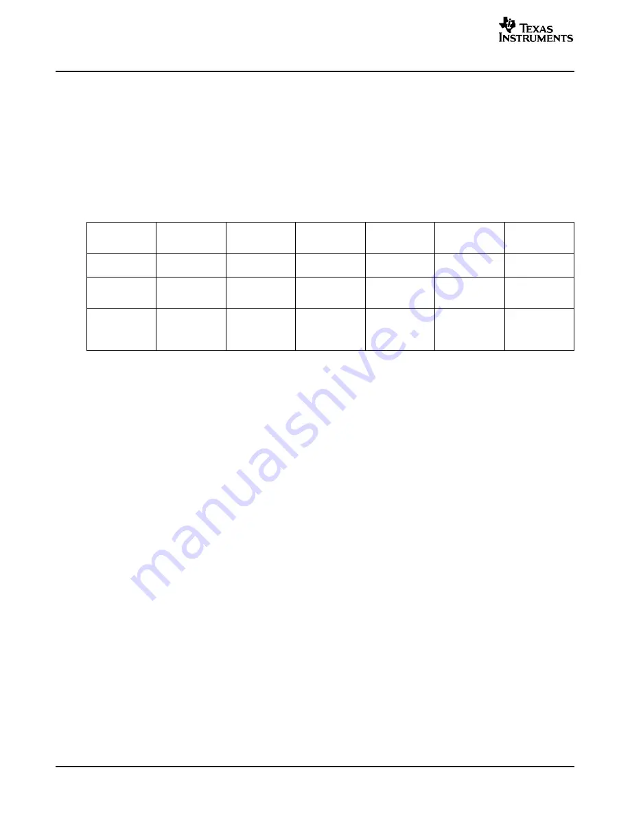
Table 4
shows the
clocking differences between the TCI6482 and the TCI100.
Table 4. Clocking Differences between TCI6482 and TCI100
Device
PLL Type
Input Clock
Frequency
Program
Clock Input
Purpose
Range
Multiplication
Multiplier via
Source
Factors
TCI100
Analog PLL
42MHz -
x1, x6, x12, x20
HW config
External clock
CPU clock
75MHz
(1)
input
TCI6482
Analog PLL
33 MHz -
x15, x20, x25,
SW config
External clock
CPU clock
(Main device
66MHz
(2) (1)
x30, x32
input
clock)
TCI6482
Analog PLL
12.5MHz -
x10
N/A
External clock
DDR2 and
(Used for DDR2
26MHz
input
Ethernet (except
and EMAC
MII)
(3)
clocking)
(1)
Supported frequency range and multipliers may change. Refer to the data manual for the latest information.
(2)
Clock range is limited to 50MHz if using PCI or SerialRapidIO boot modes.
(3)
In silicon version 2.0 and all subsequent versions this PLL is not required for RMII operation.
The PLL1 controller powers up in bypass (x1) mode with PLL1 in reset. Some boot modes change this
multiplier (see
Section 5.6
). After the PLL1 is out of reset and running, changing the PLL1 controller
multiplier and divider values (or the reference clock frequency) involves using the PLL reset mode to clear
the lock condition.
The PLL reset mode is used under the following conditions:
•
After power is applied, the PLL is automatically placed in reset mode
•
To change the input frequency (CLKIN1)
•
To change the value in any divider or multiplier register
The procedures for changing the PLL are described in
Section 6.1.3
and
Section 6.2
.
The following process should be followed to set the PLL multiplier after power-on reset. The wait times are
conservative durations to guarantee proper operation.
1. Allow PLL1 to become stable, see the device data manual for stabilization time.
2. Program PLLCTL.PLLENSRC=0 to enable the PLLCTL.PLLEN bit.
3. Program PREDIV, PLLM for the desired multiplier and divider.
4. Set PLLRST=0 to de-assert PLL reset.
5. Wait for 3000 CLKIN1 cycles for the PLL to lock.
6. Set PLLEN=1 to switch from Bypass mode to PLL mode.
TMS320TCI6482 Design Guide and Migration from TMS320TCI100
8
SPRAAC7B – April 2006
Submit Documentation Feedback


