44
11. Video Process - HA-3 and RA-5A Chassis
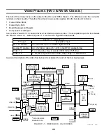
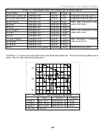
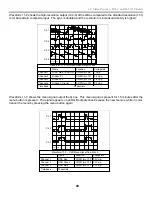
Chart 11-3 - Horizontal Sync Levels – Input is 15.735kHz NTSC at Video 1
Location
Board
Description
Frequency
Vp-p
CN005/pin A8
B
Output - Main H from B board
15.735kHz
3.5Vp-p
CN005/pin A4
B
Output - Sub H from B board
15.735kHz
3.6Vp-p
CN8801/pin A6 QM
Output – Pix sync from MID circuit
33.75kHz
3.7Vp-p
CN001/pin C18
B
Output – Final pix sync from QM bd or Video
5 or 6, 1080i input signal
33.75kHz
5Vp-p
Board Replacement Repairs
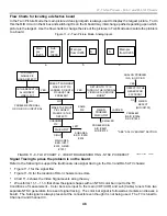
The following are very simplified signal flow diagrams used to quickly see the Main, Twin and HD signal paths
for board isolation. The paths are the same in the HA-3 and RA-5A TV chassis because they use the same B
and Q box that houses the bulk of the video signal processing.
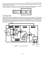
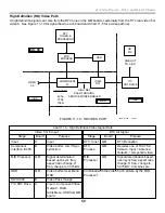
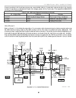
Main Video Path
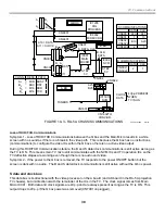
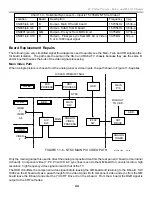
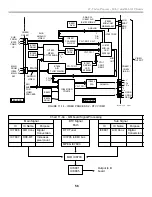
When a single picture is chosen from the analog tuner or video inputs, the path shown in Figure 11-6 applies.
Only the main signal path is used to direct the analog composite video from the rear panel (U board) or main tuner
(A board). Component video (Y, Pb, Pr) with H & V sync lines is sent to the QM board for conversion into a high
resolution, high frequency video signal to match that of the TV.
The OSD IC buffers the component video signal before leaving the QM board and returning to the B board. SW
IC002 on the B board acts as a pass-through for the video signal. Both component video and sync from the QM
board leave the B board and enter the Y/C CRT Drive IC on the A board. From the A board, the RGB signal is
output to the CRT cathodes.
OSD
DRC
PROCESS
ANALOG
VIDEO
PROCESS
IC002
SW.
ANALOG
TUNER
CRT
DRIVE
MAIN
PIX
A/V
SW.
MAIN
SW.
MID
PROCESS
RGB OUT
TO C BD.
VIDEO
1,
VIDEO
3-6
VIDEO
2
NTSC
MAIN
Hi SCAN VIDEO/33.75kHz
QM BD.
U BD.
HD BD.
B BD.
A BD.
9/4/01
8TVP12 1325
FIGURE 11-6 - NTSC MAIN PIX VIDEO PATH
Содержание KD-34XBR2 - 34" Hdtv Fd Trinitron Wega
Страница 77: ...74 RA 5A Chassis Board Layout ...
Страница 108: ...APPENDIX ...

