


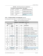
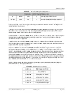


There are only two per-component registers specified so far, the debug interrupt signal (register
0) and the halt notification register (register 1), resulting in the following four possible write
actions.
Address Written
Action
0x100
Clear debug interrupt signal going to component
0x104
Set debug interrupt signal going to component
0x108
Clear halt notification from component
0x10C
Set halt notification from component
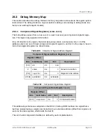
20.3.2
Debug RAM (
0x400
–
0x43f
)
SiFive systems provide at least the minimal required amount of Debug RAM, which is 28 bytes
for an RV32 system and 64 bytes for an RV64 system.
20.3.3
Debug ROM (
0x800
–
0xFFF
)
This ROM region holds the debug routines on SiFive systems. The actual total size may vary
between implementations.
Table 102:
Possible Write Actions
Chapter 20 Debug
SiFive FE310-G000 Manual: v3p2
© SiFive, Inc.
Page 111
Содержание FE310-G000
Страница 1: ...SiFive FE310 G000 Manual v3p2 SiFive Inc ...