20.3
Debug Memory Map
This section describes the debug module’s memory map when accessed via the regular system
interconnect. The debug module is only accessible to debug code running in debug mode on a
hart (or via a debug transport module).
20.3.1
Component Signal Registers (
0x100
–
0x1FF
)
The 8-bit address space from
0x100
–
0x1FF
is used to access per-component single-bit regis-
ters. This region only supports 32-bit writes.
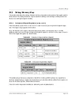
On a 32-bit write to this region, the 32-bit data value selects a component, bits 7–3 of the
address select one out of 32 per-component single-bit registers, and bit 2 is the value to be writ-
ten to that single-bit register, as shown below.
Component Signal Address Register (
csra
)
Register Offset
Bits
Field Name
Attr.
Rst.
Description
[1:0]
00
RO
0x0
2
value
RW
X
Value to be written
[7:3]
register
RW
X
Register to be written
[31:8]
0x000001
RW
0x000001
Component Signal Data Register (
csrd
)
Register Offset
Bits
Field Name
Attr.
Rst.
Description
[31:0]
component
RW
X
Component select
This addressing scheme was adopted so that RISC-V debug ROM routines can signal that a
hart has stopped using a single store instruction to an absolute address (offset from register
x0
)
and one free data register, which holds the hart ID.
The set of valid component identifiers is defined by each implementation.
Table 100:
Component Signal Address Register
Table 101:
Component Signal Data Register
Chapter 20 Debug
SiFive FE310-G000 Manual: v3p2
© SiFive, Inc.
Page 110
Содержание FE310-G000
Страница 1: ...SiFive FE310 G000 Manual v3p2 SiFive Inc ...

