


S3C2416X RISC MICROPROCESSOR
IIC-BUS INTERFACE
17-3
1.1 IIC-BUS INTERFACE
The S3C2416 IIC-bus interface has four operation modes:
•
Master transmitter mode
•
Master receive mode
•
Slave transmitter mode
•
Slave receive mode
Functional relationships among these operating modes are described below.
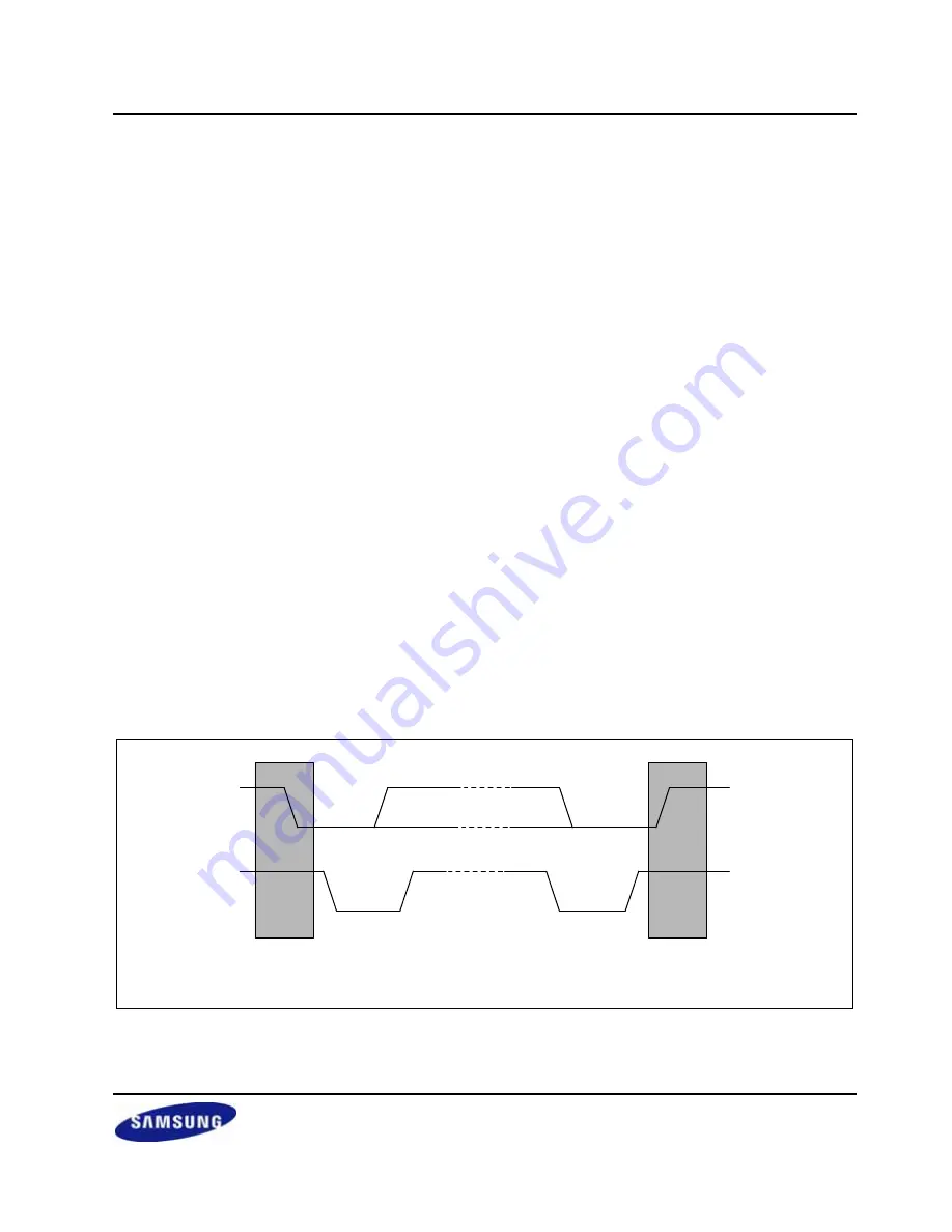
1.2 START AND STOP CONDITIONS
When the IIC-bus interface is inactive, it is usually in Slave mode. In other words, the interface should be in Slave
mode before detecting a Start condition on the SDA line (a Start condition can be initiated with a High-to-Low
transition of the SDA line while the clock signal of SCL is High). When the interface state is changed to Master
mode, a data transfer on the SDA line can be initiated and SCL signal generated.
A Start condition can transfer a one-byte serial data over the SDA line, and a Stop condition can terminate the
data transfer. A Stop condition is a Low-to-High transition of the SDA line while SCL is High. Start and Stop
conditions are always generated by the master. The IIC-bus gets busy when a Start condition is generated. A
Stop condition will make the IIC-bus free.
When a master initiates a Start condition, it should send a slave address to notify the slave device. One byte of
address field consists of a 7-bit address and a 1-bit transfer direction indicator (showing write or read).
If bit 8 is 0, it indicates a write operation (transmit operation); if bit 8 is 1, it indicates a request for data read
(receive operation).
The master will complete the transfer operation by transmitting a Stop condition. If the master wants to continue
the data transmission to the bus, it should generate another Start condition as well as a slave address. In this
way, the read-write operation can be performed in various formats.
SCL
SDA
SDA
SCL
Start
Condition
Stop
Condition
Figure 17-2. Start and Stop Condition
Содержание S3C2416
Страница 33: ...S3C2416X RISC MICROPROCESSOR PRODUCT OVERVIEW 1 5 3 BLOCK DIAGRAM Figure 1 1 S3C2416X Block Diagram ...
Страница 38: ...PRODUCT OVERVIEW S3C2416X RISC MICROPROCESSOR 1 10 153 AIN 1 U14 195 EINT 10 GPG2 K15 237 SDATA 14 C18 ...
Страница 122: ...BUS MATRIX EBI S3C2416X RISC MICROPROCESSOR 3 4 NOTES ...
Страница 204: ...DMA CONTROLLER S3C2416X RISC MICROPROCESSOR 8 18 NOTES ...
Страница 284: ...WATCHDOG TIMER S3C2416X RISC MICROPROCESSOR 11 6 NOTES ...
Страница 320: ...REAL TIME CLOCK S3C2416X RISC MICROPROCESSOR 13 16 NOTES ...
Страница 344: ...UART S3C2416X RISC MICROPROCESSOR 14 24 NOTES ...
Страница 380: ...USB2 0 DEVICE S3C2416X RISC MICROPROCESSOR 16 34 NOTES ...
Страница 432: ...2D S3C2416X RISC MICROPROCESSOR 18 38 NOTES ...
Страница 446: ...HS_SPI CONTROLLER S3C2416X RISC MICROPROCESSOR 19 14 NOTES ...
Страница 455: ...S3C2416X RISC MICROPROCESSOR HSMMC CONTROLLER 20 9 4 9 SD COMMAND ISSUE SEQUENCE Figure 20 9 Timeout Setting Sequence ...
Страница 604: ...S3C2416X RISC MICROPROCESSOR S3C2416X RISC MICROPROCESSOR 23 22 NOTES ...
Страница 638: ...PCM AUDIO INTERFACE S3C2416X RISC MICROPROCESSOR 25 18 NOTES ...
Страница 653: ...S3C2416X RISC MICROPROCESSOR ELECTRICAL DATA 26 15 Figure 26 14 SDRAM READ WRITE Timing Trp 2 Trcd 2 Tcl 2 DW 16 bit ...
Страница 670: ...ELECTRICAL DATA S3C2416X RISC MICROPROCESSOR 26 32 NOTES ...
Страница 672: ...MECHANICAL DATA S3C2416X RISC MICROPROCESSOR 30 2 Figure 27 2 330 FBGA 1414 Package Dimension 2 Bottom View ...


