MS51
Nov. 28, 2019
Page
322
of 491
Rev 1.00
MS51
32K
SE
RIES
TE
CHNICAL RE
F
EREN
CE MA
N
UAL
P0G0
P0G1
P0G2
P0G3
P0G4
P0G5
FBINEN
(PWM0CON1.3)
PWM0 and Fault Brake output control
PWM
mode
select
PWMMOD[1:0]
(PWM0CON1[7:6])
Dead
time
insertion
PWM0DTEN,
PWM0DTCNT
Mask
output
PMD0
PMEN0
PMD1
PMEN1
Brake
control
PWM
polarity
Brake event
(FB0)
P0G0_DT
P0G1_DT
PWM0C
0/1
mode
PWM0C
0/1
dead
time
FBD0
FBD1
PNP0
PNP1
PMD2
PMEN2
PMD3
PMEN3
P0G2_DT
P0G3_DT
PWM0C
2/3
mode
PWM0C
2/3
dead
time
FBD2
FBD3
PNP2
PNP3
PMD4
PMEN4
PMD5
PMEN5
P0G4_DT
P0G5_DT
PWM0C
4/5
mode
PWM0C
4/5
dead
time
FBD4
FBD5
PNP4
PNP5
BRK
0
1
0
1
0
1
0
1
0
1
0
1
0
1
0
1
0
1
0
1
0
1
0
1
0
1
0
1
0
1
0
1
0
1
0
1
PWM0MEN,
PWM0MD
PWM0FBD
PWM0PNP
PWM0_CH0
PWM0_CH3
PWM0_CH1
PWM0_CH2
PWM0_CH5
PWM0_CH4
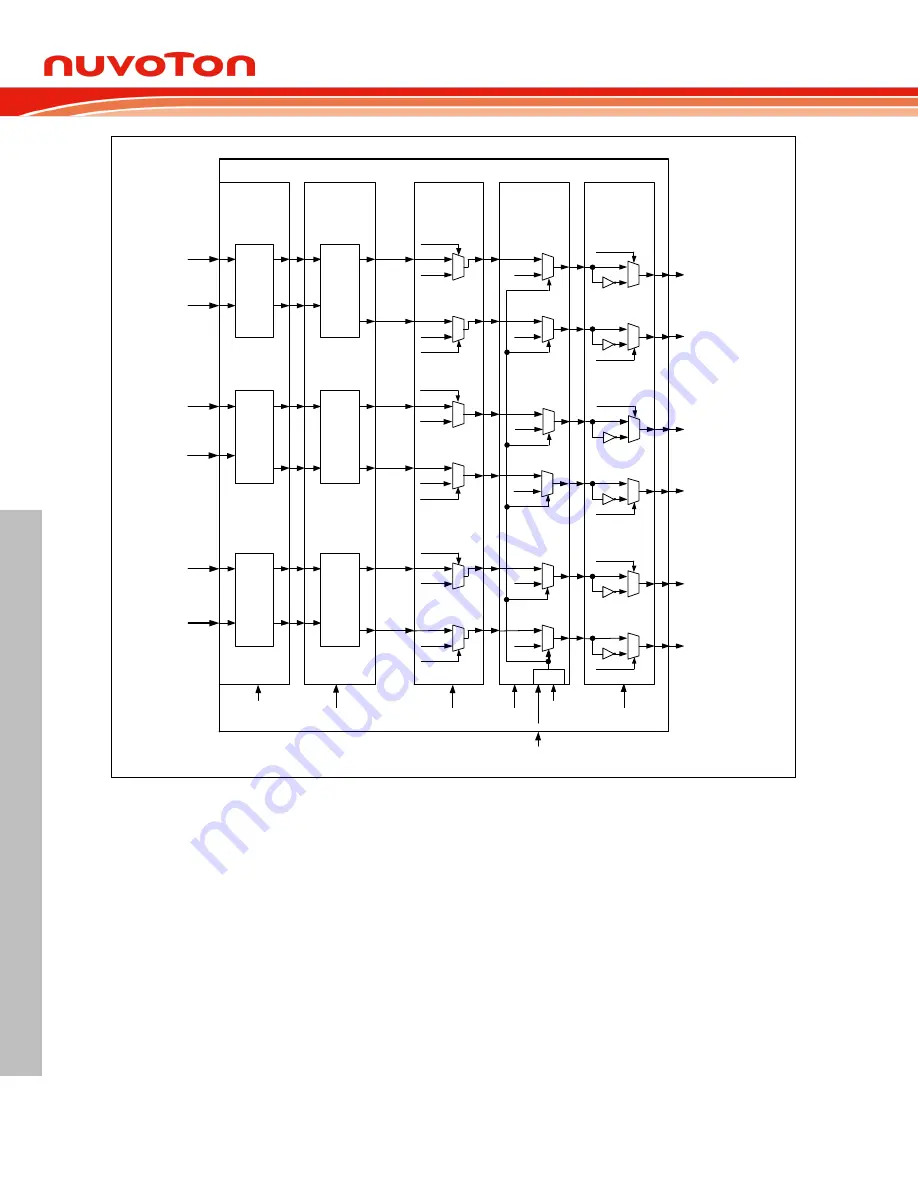
Figure 6.6-3 PWM0 and Fault Brake Output Control Block Diagram
User should follow the initialization steps below to start generating the PWM signal output. In the first
step by setting CLRPWM (PWMnCON0.4), it ensures the 16-bit up counter reset for the accuracy of
the first duration. After initialization and setting {PWMnPH, PWMnPL} and all {PWMnCxH, PWMnCxL}
registers, PWMnRUN can be set as logic 1 to trigger the 16-bit counter running. PWM starts to
generate waveform on its output pins. The hardware for all period and duty control registers are
double buffered designed. Therefore, {PWMnPH, PWMnPL} and all {PWMnCxH, PWMnCxL} registers
can be written to at any time, but the period and duty cycle of PWM will not be updated immediately
until the LOAD (PWMnCON0.6) is set and previous period is complete. This
prevents glitches
when
updating the PWM period or duty.


