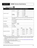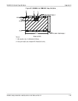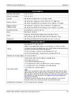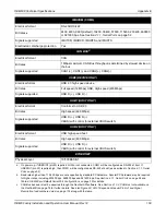
OEM638 Technical Specifications
Appendix E
OEM6 Family Installation and Operation User Manual Rev 12
176
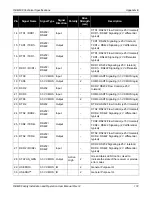
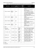
31 SPI4_nCS0
3.3V CMOS Output
Active
Low
2
Serial Peripheral Interface #4, Chip
Select 0.
33 SPI4_SCLK
3.3V CMOS Output
-
2
Serial Peripheral Interface #4, Serial
Clock.
35 SPI4_MOSI
3.3V CMOS Output
-
2
Serial Peripheral Interface #4, Master
Out / Slave In
37 SPI4_MISO
3.3V CMOS Input
-
-
Serial Peripheral Interface #4, Master
In / Slave Out
39 GND
-
-
41 I2C2_SDA
Open Drain
IO
-
-
I
2
C Interface #2, internally pulled to 3.3
V
43 I2C2_SCL
Open Drain
IO
-
-
45 GND
-
-
47 TXD5
3.3V CMOS Output
-
2
COM5 UART Signaling (3.3 V CMOS
logic)
49 RXD5
3.3V CMOS Input
-
-
COM5 UART Signaling (3.3 V CMOS
logic)
51 RTS5
3.3V CMOS Output
-
2
COM5 UART Signaling (3.3 V CMOS
logic)
53 CTS5
3.3V CMOS Input
-
-
COM5 UART Signaling (3.3 V CMOS
logic)
55 GND
-
-
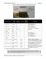
57 SDIO1_CMD
1.8V-3.0V
MMC
Output
-
12
SDIO / MMC Interface (Reserved for
internal use only. Not available
through API)
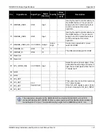
These pins are NOT 3.3 V
tolerant! Connection to 3.3 V signals
will damage the receiver.
59 SDIO1_CLK
1.8V-3.0V
MMC
Output
-
12
61 SDIO1_DAT0
1.8V-3.0V
MMC
IO
-
12
63 SDIO1_DAT1
1.8V-3.0V
MMC
IO
-
12
65 SDIO1_DAT2
1.8V-3.0V
MMC
IO
-
12
67 SDIO1_DAT3
1.8V-3.0V
MMC
IO
-
12
69 GND
-
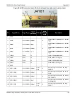
71 HSUSB0_UID
USB
IO
-
-
USB0 IDentification. Leave floating for
normal operation
Pin
Signal Name
Signal Type
Signal
Direction
Polarity
Drive
Strength
(mA)
Description

