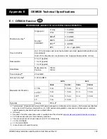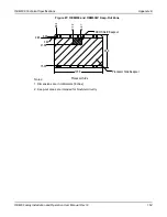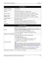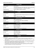
OEM628 Technical Specifications
Appendix D
OEM6 Family Installation and Operation User Manual Rev 12
158
D.1.4
USB Interface
The OEM628 includes one USB 2.0 full speed (12 Mbps) / low speed (1.5 Mbps) interface.
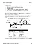
For signal integrity and EMI reasons, route differential data traces as a 90
Ω
differential pair. A small value
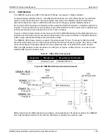
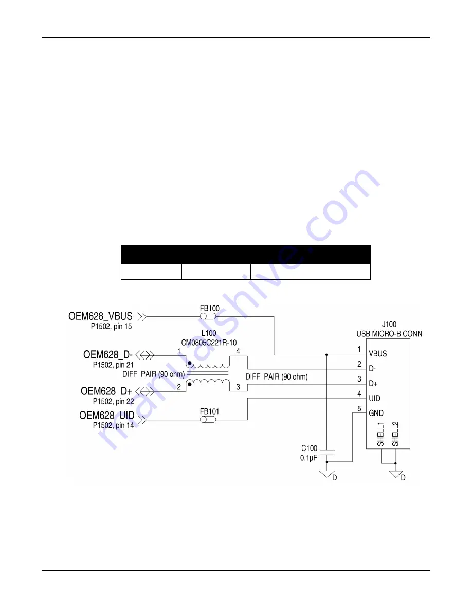
common mode choke (as shown in the figure below) may improve the radiated emissions performance.
Small ferrite beads are shown on VBUS and UID lines as a contingency against radiated emissions.
As long as the 90
Ω
impedance is maintained while routing the USB D+/D- signals, no matching resistors are
required. The pull resistors for mode selection are part of the USB PHY on the receiver card (no external pull
resistors are required on the data lines to set host or device modes).
There is an ESD protection device on the receiver card for the USB differential pair. An additional device may
be added near the USB connector but care should be taken not to cause a mismatch on the differential pair—
stubs or large capacitance ESD protection should be avoided.
The OEM628_VBUS trace should be capable of handling at least 100 mA. The traces for VBUS and UID
should be routed away from any high current switching nets and high frequency signals. The common mode
choke, ferrite beads and bypass capacitor should be placed as close as possible to the USB connector.
When the USB interface is used as a device, the UID (pin 14) may be omitted (left as a no connect) and a
standard USB Type-B connector used.
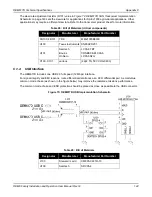
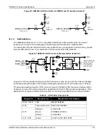
Table 34: USB Critical Components
Figure 83: OEM628 USB Implementation Schematic
ESD protection for the differential pair is provided by a low capacitance TVS device located on the OEM628
card. External ESD protection for the UID and VBUS pins is required if the pins are used.
Designator
Manufacturer
Manufacturer Part Number
L100
Steward / Laird
CM0805C221R-10

