


INTERFACE CONNECTIONS
PAGE
|
59
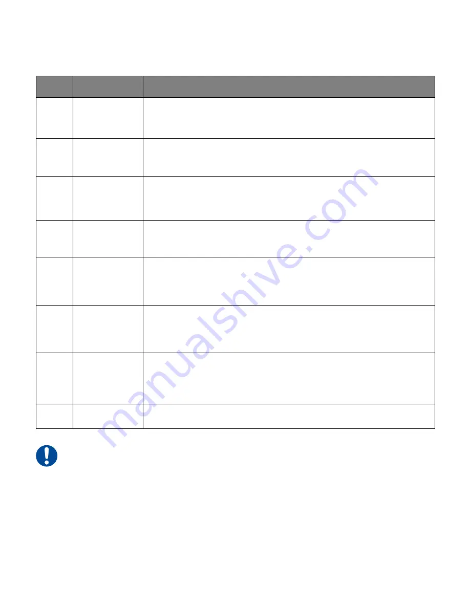
Table 3-6 Interface B (RJ45) pin descriptions
Important Note:
When swi5 VDC to the Laser Enable input on Pin 7 through a switch or
relay contact, we highly recommend adding a 100 Ohm, 1/4-watt resister in series between the
switching device and the Laser Enable input.
Pin
Function
Description
1
PWM Positive
input
Use this optoisolated voltage input for tickle and PWM signals referenced
to PWM Negative (Pin 6). The tickle signal is a +5 VDC, 1
μ
s pulse at 5 kHz
while the PWM Command signal is a +5 VDC, 5 kHz nominal (100 kHz
max) pulse width modulated square wave.
2
DC Out output
This connection provides a +15 VDC, 250 mA maximum user output
voltage referenced to GND (Pin 8).
3
Laser OK
output
This output is logic high (+5 V) when no faults are detected. The output is
low (0 V) if a fault occurs (RDY or PWR indicators flashing). The Laser OK
output sources 20 mA typical, 40 mA maximum.
4
Temperature
OK output
This output is logic high (+5 V) when laser temperature is within
operating limits. The output is low (0 V) when an over temperature
condition is detected (RDY indicator flashing continuously). The
Temperature OK output sources 20 mA typical, 40 mA maximum.
5
Voltage OK
output
This output is logic high (+5 V) when DC input voltage is within limits. The
output is low (0 V) if the DC input voltage is under or over voltage limits
and the PWR indicator flashes a repeating sequence of 1 blink (under
voltage) or 2 blinks (overvoltage). The Voltage OK output sources 20 mA
typical, 40 mA maximum.
6
PWM Negative
input
This input provides the negative, or return, side of the optoisolated
tickle/PWM Command signal referenced to PWM Positive (Pin 1). If this pin
does not provide a PWM return, it must be connected to GND (Pin 8). The
control board will be damaged if this pin is left unconnected.
7
Laser Enable
input
When this input is logic high (+5 V), the laser is enabled (RDY indicator
illuminates yellow). The laser is disabled when the input is low (0 V). Tickle
or PWM signals are applied to the RF circuit immediately after this input
goes high.
8
GND
This connection is the ground, or return, reference for all RJ45 inputs and
outputs.
Содержание v30
Страница 1: ...ENGINEERED BY SYNRAD v30 Laser User Manual...
Страница 16: ...OEM V30 LASER LABEL LOCATIONS PAGE 16 OEM v30 Laser label locations...
Страница 22: ...DECLARATION OF CONFORMITY PAGE 22 Declaration of conformity Figure 2 Declaration Document...
Страница 64: ...INTERFACE CONNECTIONS PAGE 64 Figure 3 16 Laser OK output to PLC input...
Страница 90: ...BEAM DELIVERY OPTICS PAGE 90 This page is left blank intentionally...
Страница 100: ...INDEX PAGE 1 This page is intentionally left blank...