Pro I: Signal Conditioning and Interface Modules
Pro-Inter-SL Rev. A
ADwin
184
ADwin-Pro
Hardware, manual version 2.9, June 2006
5.9.9 Pro-Inter-SL Rev. A
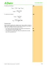
General information about this fieldbus module is given in
,
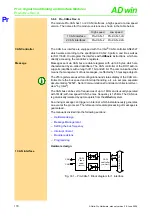
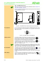
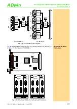
shows the side-view (printed circuit board) and the front panel of the
Pro-Inter-SL module.
Fig. 317 – Pro-INTER-SL: Printed circuit board and front panel
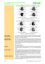
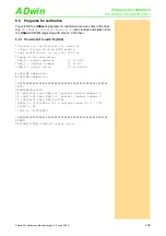
Pin assignment
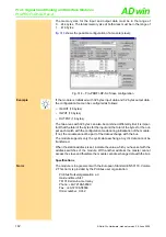
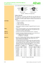
shows the pin assignment of the D-SUB sockets for the connection of
the Interbus (input and output).
Fig. 318 – Pro-INTER-SL: Pin assignment
Status display
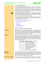
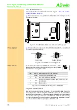
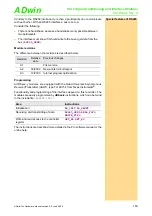
On the front panel of the Pro-INTER-SL module are 4 status
LEDs, which inform about the module communication. Table 6
illustrates the meaning of the LEDs:
Fig. 319 – Pro-INTER-SL: Meaning of the status LED
Integration into the Interbus
After having connected the bus (hardware), the master will be able to read the
bus configuration. After reading the master has all necessary information
about the connected slaves. For example the size of the input and output areas
for cyclic data exchange and the size of the PCP communication. After reading
the bus configuration the communication can be started immediately. More-
over, the master identifies the participants (DIO, PC, AIN, ...).
INTER-SL
INTE
RB
US
IN
1
BA
CC
TR
INT
ERBUS OUT
RBDA
19PROFI1
OCX
16MHz
FPGA
A42MX16
ON
DIP
1
2
3
4
5
6
7
8
74LS19
DCP010505BP
74HC123
IS61C256
TH 1055
Input (male)
Output (female)
5
4
3
2
1
9
8
7
6
/DI1
/DO1
GND
DI1
DO1
RESERVED
RESERVED
/DO2
/DI2
RESERVED
RBST
1
2
3
4
5
6
7
8
9
DO2
DI2
GND
RESERVED
GND
LED
Name Meaning when the LED is active
1
RBDA Interbus output is switched off.
2
TR
PCP communication is active.
3
CC
Physical connection to the master, master will not
be initialized.
4
BA
Bus is active.
BA
CC
TR
RBDA

