ADwin-Pro
Hardware, manual version 2.9, June 2006
81
Pro I: Analog Output Modules
Pro-AOut-8/16 Rev. A
ADwin
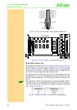
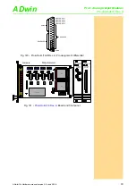
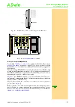
Fig. 144 – Pro-AOut-8/16-D Rev. A: Pin assignment differential
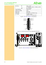
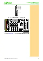
Fig. 145 –
: Board
Setting the Output Voltage Range
The module
is equipped with 4 DAC, the module
with 8 DAC. The DAC 1 to 4 are on the base PCB and
the DAC 5 to 8 are mounted on an additional PCB which will be plugged into
the base PCB.
The output voltage of the DAC can be set by two jumpers. As a default setting
all DAC are set to the voltage range of ± 10V. If you want to adjust the DAC 1
to 4 on the base PCB of the output module Pro-AOut-8/16 you have to remove
the additional PCB which is fixed by two screws.
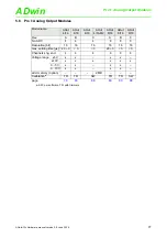
all possibilities to adjust the jumpers are listed The "x" in the poten-
tiometer title stands for the number of the corresponding DAC (see PCB
imprint near to the potentiometers).
The potentiometers U0x, Bx and Gainx are used for an accurate adjustment of
gain and offset (
).
If nothing else has been said on ordering the module, the voltage range is set
to ±10V. After every jumper setting you have to recalibrate the DAC, in order
to assure correct measurement results. The individual steps are described in
chapter 6.3.1 "Calibration per Software"
ANALOG OUT 1
ANALOG OUT 2
ANALOG OUT 3
ANALOG OUT 4
ANALOG OUT 5
ANALOG OUT 6
ANALOG OUT 7
ANALOG OUT 8
DGND
19
18
17
16
15
14
13
12
11
10
9
8
7
6
5
4
3
2
1
37
36
35
34
33
32
31
30
29
28
27
26
25
24
23
22
21
20
AGND
RESERVED
RESERVED
19DA714
FPGA
FPGA
ON
1 2 3 4 5 6 7 8
A0 A1 A2 A3 A4 A5 A6 A7
LS19
OCX
DC/DC-converter
LS
125
LS
125
LS
125
LS
125
DAC7
1
4
20V
BIP
UO4 BO4 G4
10V
UNI
031
DAC7
1
4
20V
BIP
UO3 BO3 G3
10V
UNI
031
DAC7
1
4
20V
BIP
UO2 BO2 G2
10V
UNI
031
DAC7
1
4
20V
BIP
UO1 BO1 G1
10V
UNI
031
1
2
3
4
DC/DC-converter
LS
125
LS
125
LS
125
LS
125
DAC7
1
4
20V
BIP
UO8 BO8 G8
10V
UNI
031
DAC7
1
4
20V
BIP
UO7 BO7 G7
10V
UNI
031
DAC7
1
4
20V
BIP
UO6 BO6 G6
10V
UNI
031
DAC7
1
4
20V
BIP
UO5 BO5 G5
10V
UNI
031
5
6
7
8
Potentiometers
Jumpers


