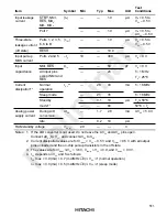
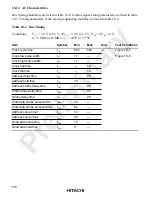


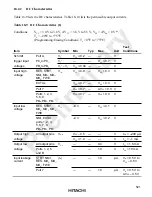


522
Item
Symbol
Min
Typ
Max
Uni t
Test
Conditions
Three-state
leakage current
(off state)
Ports 1, 2, 3,
5, 6, 8 to B
|I
TSI
|
—
—
1.0
µ
A
V
in
= 0.5 V to
V
CC
– 0.5 V
Input pull-up
MOS current
Ports 2 and 5
–I
p
10
—
300
µ
A
V
in
= 0 V
Input
NMI,
RES
C
in
—
—
50
pF
V
in
= 0 V
capacitance
All input pins
except NMI and
RES
—
—
20
f = 1 MHz
T
a
= 25
°
C
Current
dissipation
*
2
*
4
Normal
operation
I
CC
*
4
—
28
48
mA
f = 18 MHz
Sleep mode
—
21
35
f = 18 MHz
Standby
—
0.1
10
µ
A
T
a
≤
50
°
C
mode
*
3
—
—
80
50
°
C < T
a
Analog power
supply current
During A/D
conversion
AI
CC
—
1.7
2.8
mA
Idle
—
0.2
10
µ
A
RAM standby voltage
V
RAM
2.0
—
—
V
Notes: 1. If the A/D converter is not used, do not leave the AV
CC
and AV
SS
pins open.
Connect AV
CC
to V
CC
, and connect AV
SS
to V
SS
.
2. Current dissipation values are for V
IHmin
= V
CC
– 0.5 V and V
ILmax
= 0.5 V with all output
pins unloaded and the on-chip pull-up transistors in the off state.
3. The values are for V
RAM
≤
V
CC
< 3.6 V, V
IHmin
= V
CC
×
0.9, and V
ILmax
= 0.3 V.
4. I
CC
depends on V
CC
and f as follows:
I
CC
max = 3.0 (mA) + 0.7 (mA/MHz
⋅
V)
×
V
CC
×
f (normal operation)
I
CC
max = 3.0 (mA) + 0.5 (mA/MHz
⋅
V)
×
V
CC
×
f (sleep mode)
Power supply current value when programming/erasing in flash memory (T
a
= 0
°
C to
+75
°
C) is
20
mA (max) higher than the power supply current value in normal operation.