446
15.5.4
Erase Block Register 2 (EBR2)
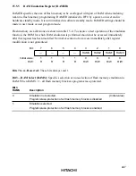
EBR2 is an 8-bit register that specifies the flash memory erase area block by block. EBR2 is
initialized to H'00 by a power-on reset, in hardware standby mode and software standby mode,
when a low level is input to the FWE pin. Bit 0 will be initialized to 0 if bit SWE of FLMCR1 is
not set, even though a high level is input to pin FWE. When a bit in EBR2 is set to 1, the
corresponding block can be erased. Other blocks are erase-protected. Only one of the bits of EBR1
and EBR2 combined can be set.
Do not set more than one bit , as this will cause all the bits in both
EBR1 and EBR2 to be automatically cleared to 0. Bits 7 to 4 are reserved and must only be written
with 0. When on-chip flash memory is disabled, a read will return H'00, and writes are invalid.
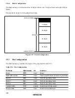
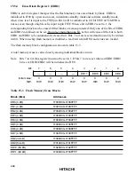
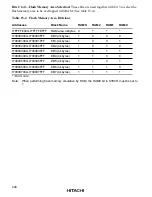
The flash memory block configuration is shown in table 15-3.
A total memory erase is carried out by erasing individual blocks in turn.
Note:
Bits 7 to 4 in this register must not be set to 1. If bits 7 to 4 are set when an EBR1/EBR2
bit is set, EBR1/EBR2 will be initialized to H'00.
Bit:
7
6
5
4
3
2
1
0
—
—
—
—
EB11
EB10
EB9
EB8
Initial value:
0
0
0
0
0
0
0
0
R/W:
R/W
R/W
R/W
R/W
R/W
R/W
R/W
R/W
Table 15-3 Flash Memory Erase Blocks
Block (Size)
Addresses
EB0 (4 kB)
H'000000–H'000FFF
EB1 (4 kB)
H'001000–H'001FFF
EB2 (4 kB)
H'002000–H'002FFF
EB3 (4 kB)
H'003000–H'003FFF
EB4 (4 kB)
H'004000–H'004FFF
EB5 (4 kB)
H'005000–H'005FFF
EB6 (4 kB)
H'006000–H'006FFF
EB7 (4 kB)
H'007000–H'007FFF
EB8 (32 kB)
H'008000–H'00FFFF
EB9 (64 kB)
H'010000–H'01FFFF
EB10 (64 kB)
H'020000–H'02FFFF
EB11 (64 kB)
H'030000–H'03FFFF

