441
15.4
Register Configuration
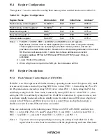
The registers *
1
used to control the on-chip flash memory when enabled are shown in table 15-2.
Table 15-2 Register Configuration
Register Name
Abbreviation
R/W
Initial Value
Address
*
2
Flash memory control register 1
FLMCR1
*
1
R/W
H'00
*
3
H'FF40
Flash memory control register 2
FLMCR2
*
1
R
H'00
H'FF41
Erase block register 1
EBR1
*
1
R/W
H'00
H'FF42
Erase block register 2
EBR2
*
1
R/W
H'00
H'FF43
RAM emulation register
RAMER
*
1
R/W
H'F0
H'FF47
Notes: 1. FLMCR1, FLMCR2, EBR1, and EBR2, and RAMER are 8-bit registers.
Byte access must be used on these registers (do not use word or longword access).
These registers are for use exclusively by the flash memory version, and are not
provided in the mask ROM version. Reads to the corresponding addresses in the mask
ROM version will always return 1, and writes to these addresses are invalid.
Access to address H'FF44 to H'FF46 and H'FF48 to H'FF4F (lower 16 bits) is
prohibited.
2. Lower 16 bits of the address.
3. When a high level is input to the FWE pin, the initial value is H'80.
15.5
Register Descriptions
15.5.1
Flash Memory Control Register 1 (FLMCR1)
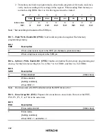
FLMCR1 is an 8-bit register used for flash memory operating mode control. Program-verify mode
or erase-verify mode is entered by setting SWE bit to 1 when FWE = 1, then setting the PV or EV
bit. Program mode is entered by setting SWE1 bit to 1 when FWE = 1, then setting the PSU bit,
and finally setting the P bit. Erase mode is entered by setting SWE bit to 1 when FWE = 1, then
setting the ESU bit, and finally setting the E bit. FLMCR1 is initialized by a power-on reset, and
in hardware standby mode and software standby mode. Its initial value is H'80 when a high level
is input to the FWE pin, and H'00 when a low level is input. When on-chip flash memory is
disabled, a read will return H'00, and writes are invalid.
Writes are enabled only in the following cases: Writes to bit SWE of FLMCR1 enabled when
FWE = 1, to bits ESU, PSU, EV, and PV when FWE = 1 and SWE = 1, to bit E when FWE = 1,
SWE = 1 and ESU = 1, and to bit P when FWE = 1, SWE = 1, and PSU = 1.
Notes: 1. To prevent erroneous programming or erasing, the setting of individual bits in this
register must be carried out in accordance with the programming and erase flowcharts.

