434
15.2
Overview
15.2.1
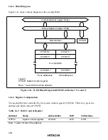
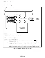
Block Diagram
Module bus
Bus interface/controller
Flash memory
(256 kbytes)
Operating
mode
FLMCR2
Internal address bus
Internal data bus (16 bits)
FWE pin
Mode pin
EBR1
EBR2
RAMER
FLMCR1
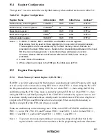
Flash memory control register 1
Flash memory control register 2
Erase block register 1
Erase block register 2
RAM emulation register
Legend
FLMCR1:
FLMCR2:
EBR1:
EBR2:
RAMER:
Notes: 1.
2.
Functions as the FWE pin in the flash memory version, and as the RESO pin in the
mask ROM version.
The registers that control the flash memory (FLMCR1, FLMCR2, EBR1, EBR2,
and RAMER) are for use exclusively by the flash memory version, and are not
provided in the mask ROM version. Reads to the corresponding addresses in the
mask ROM version will always return 1, and writes to these addresses are invalid.
*
2
*
1
*
2
*
2
*
2
*
2
Figure 15-1 Block Diagram of Flash Memory


