445
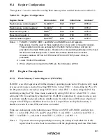
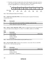
Bit 7
FLER
Description
0
Flash memory is operating normally
(Initial value)
Flash memory program/erase protection (error protection) is disabled
[Clearing condition]
RES
pin reset, WDT reset, or hardware standby mode
1
An error has occurred during flash memory programming/erasing
Flash memory program/erase protection (error protection) is enabled
[Setting condition]
•
When flash memory is read
*
2
during programming/erasing (including a vector
read or instruction fetch, but excluding reads in a RAM area overlapping flash
memory space)
•
Immediately after the start of exception handling during programming/erasing
(but excluding reset, illegal instruction, trap instruction, and division-by-zero
exception handling)
•
When a SLEEP instruction (including software standby) is executed during
programming/erasing
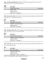
Bits 6 to 0—Reserved: Only 0 may be written to these bits.
15.5.3
Erase Block Register 1 (EBR1)
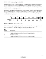
EBR1 is an 8-bit register that specifies the flash memory erase area block by block. EBR1 is
initialized to H'00 by a power-on reset, in hardware standby mode and software standby mode,
when a low level is input to the FWE pin, and when a high level is input to the FWE pin and the
SWE bit in FLMCR1 is not set. When a bit in EBR1 is set to 1, the corresponding block can be
erased. Other blocks are erase-protected. Only one of the bits of EBR1 and EBR2 combined can
be set.
Do not set more than one bit , as this will cause all the bits in both EBR1 and EBR2 to be
automatically cleared to 0. When on-chip flash memory is disabled, a read will return H'00, and
writes are invalid.
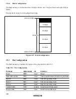
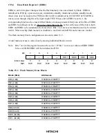
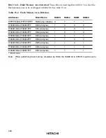
The flash memory block configuration is shown in table 15-3.
A total memory erase is carried out by erasing individual blocks in turn.
Bit:
7
6
5
4
3
2
1
0
EB7
EB6
EB5
EB4
EB3
EB2
EB1
EB0
Initial value:
0
0
0
0
0
0
0
0
R/W:
R/W
R/W
R/W
R/W
R/W
R/W
R/W
R/W


