


430
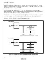
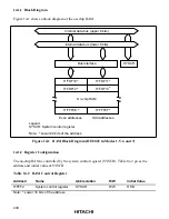
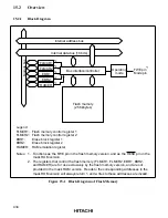
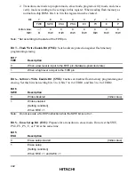
14.1.1 Block Diagram
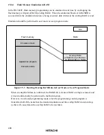
Figure 14-1 shows a block diagram of the on-chip RAM.
H'FDF10
H'FDF12
*
*
H'FFF0E
*
H'FDF11
H'FDF13
*
*
H'FFF0F
*
Bus interface
SYSCR
On-chip RAM
Even addresses
Odd addresses
Legend
SYSCR: System control register
Note:
*
Lower 20 bits of the address
Internal data bus (upper 8 bits)
Internal data bus (lower 8 bits)
Figure 14-1 RAM Block Diagram (H8/3022 in Modes 1, 5, 6 and 7)
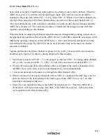
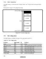
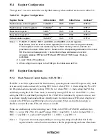
14.1.2 Register Configuration
The on-chip RAM is controlled by the system control register (SYSCR). Table 14-2 gives the
address and initial value of SYSCR.
Table 14-2 RAM Control Register
Address
*
Name
Abbreviation
R/W
Initial Value
H'FFF2
System control register
SYSCR
R/W
H'0B
Note:
*
Lower 16 bits of the address