497
17.2
Register Configuration
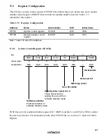
This LSI has a system control register (SYSCR) that controls the power-down state, and a module
standby control register (MSTCR) that controls the module standby function. Table 17-2
summarizes this register.
Table 17-2 Register Configuration
Address
*
Name
Abbreviation
R/W
Initial Value
H'FFF2
System control register
SYSCR
R/W
H'0B
H'FF5E
Module standby control
register
MSTCR
R/W
H'40
Note:
*
Lower 16 bits of the address.
17.2.1
System Control Register (SYSCR)
Bit
Initial value
Read/Write
7
SSBY
0
R/W
6
STS2
0
R/W
5
STS1
0
R/W
4
STS0
0
R/W
3
UE
1
R/W
0
RAME
1
R/W
2
NMIEG
0
R/W
1
—
1
—
Software standby
Enables transition to
software standby mode
RAM enable
Standby timer select 2 to 0
These bits select the
waiting time at exit from
software standby mode
User bit enable
NMI edge select
Reserved bit
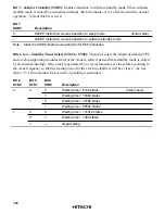
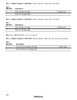
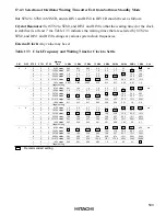
SYSCR is an 8-bit readable/writable register. Bit 7 (SSBY) and bits 6 to 4 (STS2 to STS0) control
the power-down state. For information on the other SYSCR bits, see section 3.3, System Control
Register.

