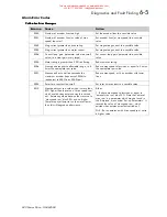
)XQFWLRQ
#
%ORFNV
##
8098
953#
9HFWRU
#
'ULYH
#0#
+$
7968;7
%/2&.
#
',$*5$0
Source
Addres
Offset
Calibration
Modulu
DIAGNOST
::ANOU
X
% To get 100%
Hardware Offset
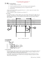
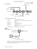
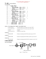
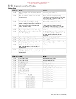
Figure 5.29 Analogue O/P Block Diagram
$1287
#4#+
&
8,#
$1'
#
$1287
#5#+
)
9,
% TO GET 10V
Scalar value which produces 10 V output.
OFFSET
Offset value added to the normal output value after the scalar and before the
modulus.
CALIBRATION
Output scalar.
MODULUS
Unsigned analogue output enable.
SOURCE TAG N°
Source of output value.
ANOUT X
Diagnostic after scaling block if source tag is non zero else it could be used as a
destination tag.
HARDWARE OFFSET
Offset value added to the final output value.
,13876
%/2&.
#
',$*5$0
Digital input Diagnostic
Value For TRUE 1
Value For FALSE 1
Destination 2
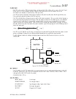
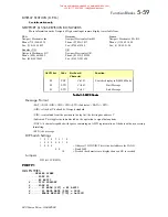
Figure 5.30 Digital Input Block Diagram
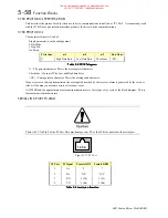
The Destination for a digital input can be any valid TAG N°; this means that a digital input can be used to select
one of two values for a given parameter. It is also possible to treat the values for TRUE and FALSE as
destination Tags from other functions or inputs.
This manual was downloaded on www.sdsdrives.com
+44 (0)117 938 1800 - [email protected]

