


enCoRe™ V CY7C643xx, enCoRe™ V LV CY7C604xx TRM, Document No. 001-32519 Rev *H
150
Full-Speed USB
20.3.6
EP0_CNT Register
The Endpoint 0 Count Register (EP0_CNT) is used to con-
figure endpoint 0.
Whenever the count updates from a setup or OUT transac-
tion, this register locks and cannot be written by the CPU.
Reading the EP0_CR register unlocks this register. This pre-
vents firmware from overwriting a status update on incoming
setup or OUT transactions, before firmware has a chance to
read the data.
Bit 7: Data Toggle.
This bit selects the data packet's toggle
state. For IN transactions, firmware must set this bit. For
OUT or setup transactions, the SIE hardware sets this bit to
the state of the received Data Toggle bit. ‘0’ is DATA0. ‘1’ is
DATA1.
Bit 6: Data Valid.
This bit indicates whether there were
errors in OUT or setup transactions. It is cleared to '0' if
CRC, bit stuff, or PID errors have occurred. This bit does not
update for some endpoint mode settings. This bit may be
cleared by writing a zero to it when the register is not locked.
‘0’ is error in data received. ‘1’ is no error.
Bits 3 to 0: Byte Count[3:0].
These bits indicate the num-
ber of data bytes in a transaction. For IN transactions, firm-
ware loads the count with the number of bytes to be
transmitted to the host from the endpoint FIFO. Valid values
are 0 to 8. For OUT or setup transactions, the count is
updated by hardware to the number of data bytes received,
plus two for the CRC bytes. Valid values are 2 to 10.
For additional information, refer to the
20.3.7
EP0_DRx Register
The Endpoint 0 Data Register (EP0_DRx) is used to read
and write data to the USB control endpoint.
The EP0_DRx registers have a hardware-locking feature
that prevents the CPU write when setup is active. The regis-
ters are locked as soon as the setup token is decoded and
remain locked throughout the setup transaction and until the
EP0_CR register has been read. This is to prevent overwrit-
ing new setup data before firmware knows it has arrived.
All other endpoint data buffers do not have this locking fea-
ture.
Bits 7 to 0: Data Byte[7:0].
These registers are shared for
both transmit and receive. The count in the EP0_CNT regis-
ter determines the number of bytes received or to be trans-
ferred.
For additional information, refer to the
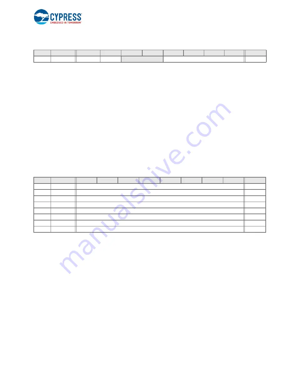
Address
Name
Bit 7
Bit 6
Bit 5
Bit 4
Bit 3
Bit 2
Bit 1
Bit 0
Access
0,37h
Data Toggle
Data Valid
Byte Count[3:0]
# : 00
Address
Name
Bit 7
Bit 6
Bit 5
Bit 4
Bit 3
Bit 2
Bit 1
Bit 0
Access
0,38h
EP0_DR0
Data Byte[7:0]
RW : 00
0,39h
EP0_DR1
Data Byte[7:0]
RW : 00
0,3Ah
EP0_DR2
Data Byte[7:0]
RW : 00
0,3Bh
EP0_DR3
Data Byte[7:0]
RW : 00
0,3Ch
EP0_DR4
Data Byte[7:0]
RW : 00
0,3Dh
EP0_DR5
Data Byte[7:0]
RW : 00
0,3Eh
EP0_DR6
Data Byte[7:0]
RW : 00
0,3Fh
EP0_DR7
Data Byte[7:0]
RW : 00


